
[Paper Review] Tunable quantum emitters on large-scale foundry silicon photonics
This paper presents a hybrid integration platform combining InAs/InP quantum dot microchiplets with large-scale 300 mm foundry silicon photonics, enabling electrically tunable single-photon emission via non-volatile Stark shifting. The system achieves individual emitter addressability, resonance fluorescence, and scalable wavelength tuning with sub-3 dB fiber coupling, paving the way for programmable, on-chip quantum processors in commercial semiconductor foundries.
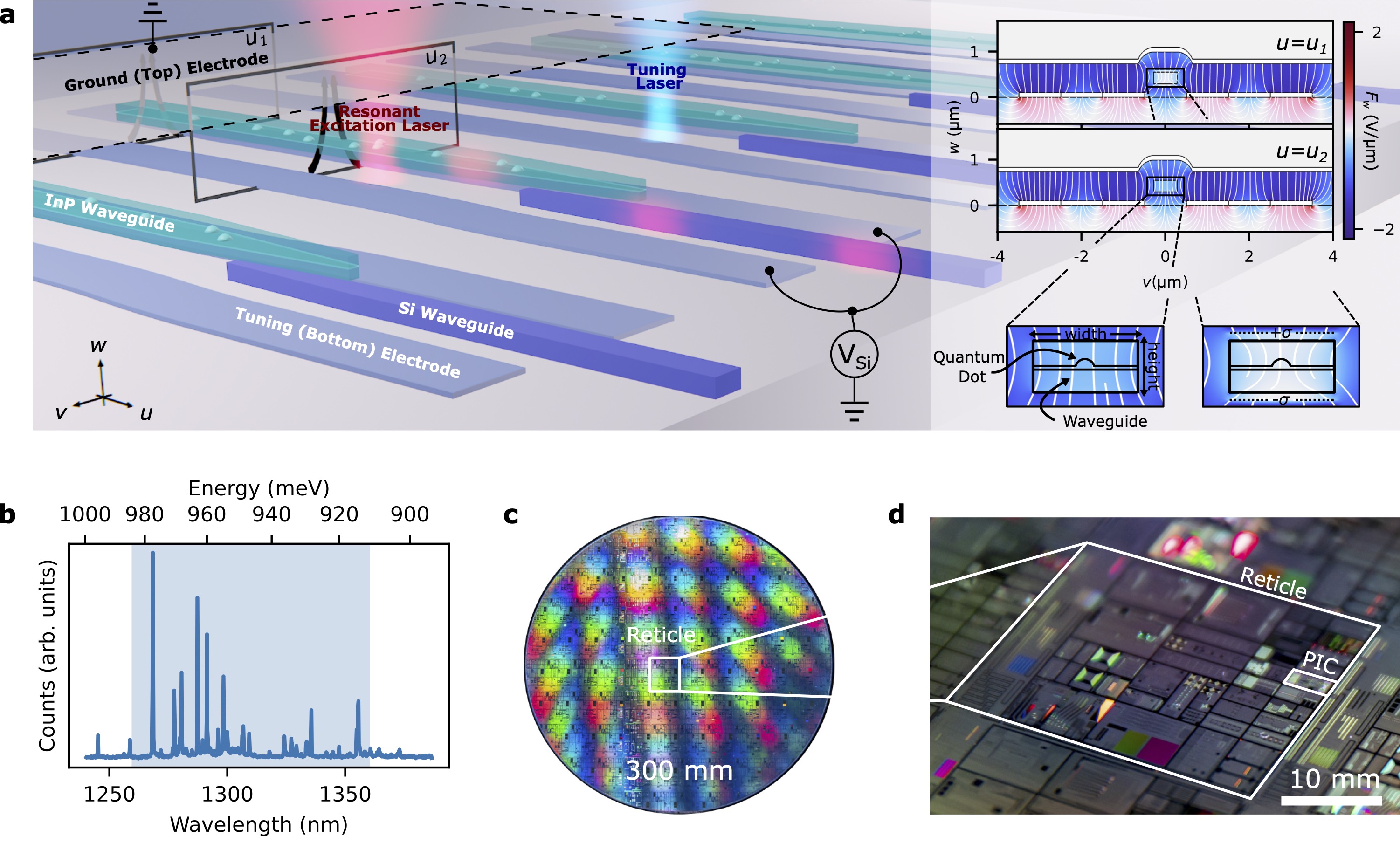
Controlling large-scale many-body quantum systems at the level of single photons and single atomic systems is a central goal in quantum information science and technology. Intensive research and development has propelled foundry-based silicon-on-insulator photonic integrated circuits to a leading platform for large-scale optical control with individual mode programmability. However, integrating atomic quantum systems with single-emitter tunability remains an open challenge. Here, we overcome this barrier through the hybrid integration of multiple InAs/InP microchiplets containing high-brightness infrared semiconductor quantum dot single photon emitters into advanced silicon-on-insulator photonic integrated circuits fabricated in a 300~mm foundry process. With this platform, we achieve single photon emission via resonance fluorescence and scalable emission wavelength tunability through an electrically controlled non-volatile memory. The combined control of photonic and quantum systems opens the door to programmable quantum information processors manufactured in leading semiconductor foundries.
Motivation & Objective
- Address the challenge of integrating tunable, single-photon emitters with large-scale photonic integrated circuits (PICs) for scalable quantum information processing.
- Overcome limitations of monolithic III-V PICs, such as high propagation losses and lack of individual emitter control, by leveraging the scalability and low loss of foundry-based silicon-on-insulator (SOI) PICs.
- Enable individual control of multiple quantum dot emitters through hybrid integration with transfer-printed InP chiplets and non-volatile electrical tuning.
- Achieve high-fidelity single-photon emission with resonance fluorescence and minimal background noise via excellent pump rejection in the SOI PIC.
- Develop a scalable, manufacturable platform compatible with commercial semiconductor foundries for future large-scale quantum photonic systems.
Proposed method
- Fabricated advanced SOI photonic integrated circuits (PICs) in a 300 mm foundry process with sub-3 dB fiber coupling efficiency using iterative design and post-processing techniques.
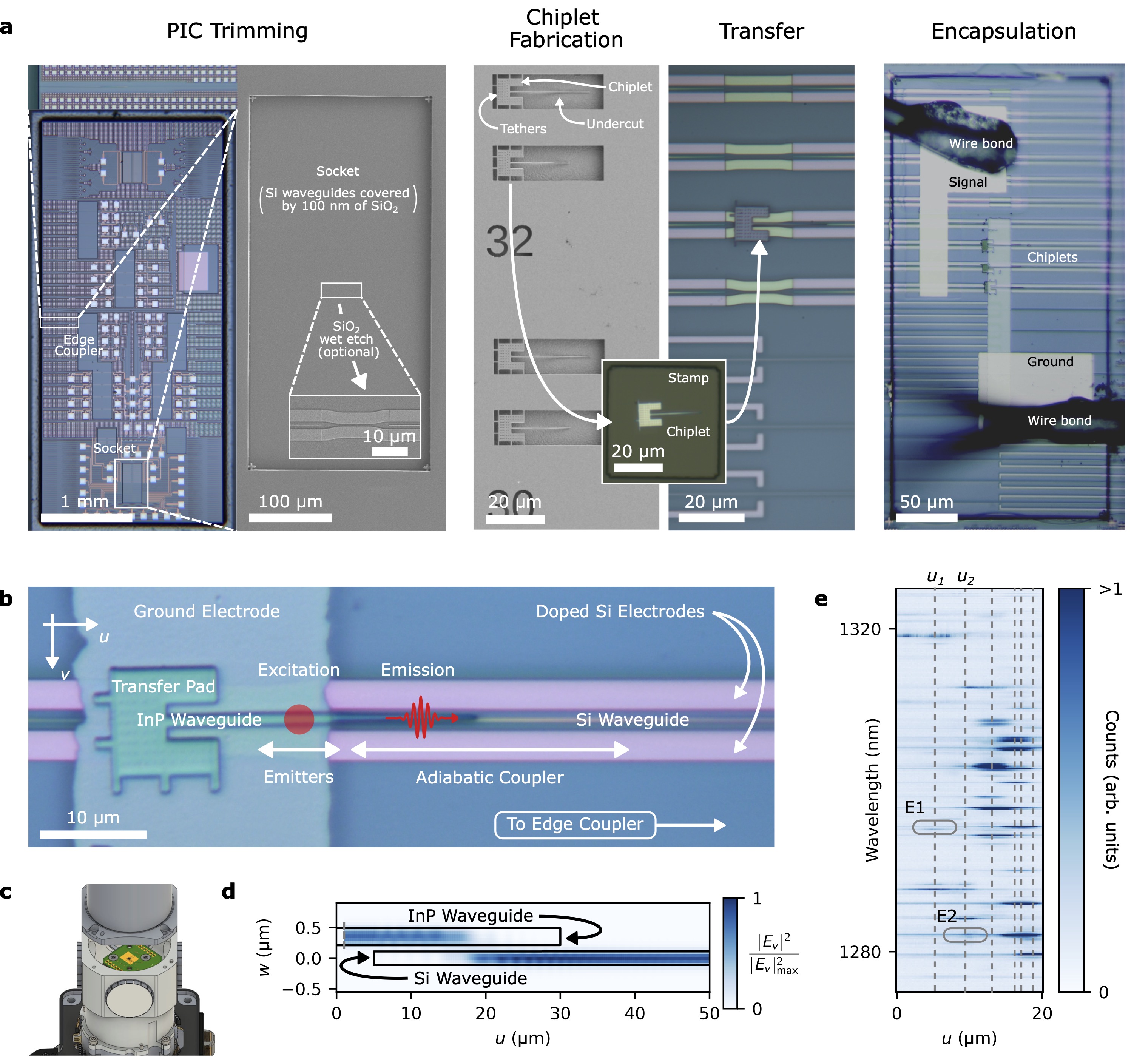
- Transfer-printed multiple InAs/InP microchiplets containing high-brightness InAs/InP quantum dots onto the SOI PIC using scalable, alignment-precise transfer printing methods.
- Employed resonant excitation via focused laser beams to achieve resonance fluorescence from individual quantum dots with high signal-to-noise ratio.
- Integrated an electrically controlled non-volatile memory structure adjacent to each quantum dot for localized Stark shifting, enabling wavelength tuning without continuous power.
- Utilized a charge-coupled tuning mechanism to induce spectral shifts via electrostatic potential modulation, achieving tunability across multiple emitters with minimal crosstalk.
- Characterized emitter performance using cross-correlation measurements (g(2)(0) < 0.65) and spectral tuning range (up to 100 GHz), validating individual control and coherence.
Experimental results
Research questions
- RQ1Can high-brightness, single-photon-emitting quantum dots be stably and precisely hybrid-integrated with large-scale, foundry-based silicon photonic circuits?
- RQ2Can individual quantum dot emitters be electrically tuned with non-volatile, localized control while maintaining high photon indistinguishability and low background noise?
- RQ3To what extent can the spectral tuning range and emitter linewidth be optimized through post-processing and device engineering?
- RQ4How scalable is the integration of multiple tunable emitters on a single PIC using transfer printing and electrical tuning?
- RQ5Can the platform support programmable, many-body quantum photonic systems with individual emitter addressability and low crosstalk?
Key findings
- The hybrid integration of InAs/InP microchiplets with 300 mm foundry SOI PICs achieved sub-3 dB fiber coupling efficiency, enabling efficient on-chip optical interfacing.
- Resonance fluorescence was observed from individual quantum dots with g(2)(0) < 0.65, confirming high single-photon purity and low multi-photon emission.
- Electrically controlled non-volatile memory enabled spectral tuning of individual emitters with a range of up to 100 GHz, demonstrating scalable, low-power wavelength control.
- The platform exhibited excellent pump rejection, allowing direct observation of resonance fluorescence without additional filtering, crucial for low-noise operation.
- Cross-talk between emitters was minimized, with g(2)(0) < 0.65 for emitters separated by ~5 µm, indicating high-fidelity individual addressing and low crosstalk.
- The integration method supports scalability, with potential for millions of addressable emitters using conventional optical microscopy and electrode arrays.
Better researchstarts right now
From reading papers to final review, dramatically reduce your research time.
No credit card · Free plan available
This review was created by AI and reviewed by human editors.