
[Paper Review] Femtosecond laser induced creation of G and W-centers in silicon-on-insulator substrates
This study demonstrates the deterministic, on-demand creation of W- and G-centers—silicon-based quantum emitters—in silicon-on-insulator (SOI) substrates using femtosecond laser annealing. The method achieves defect quality comparable to conventional implantation techniques, enables creation without carbon implantation, and allows selective erasure of G-centers while enhancing W-center emission via low-temperature annealing, enabling precise, localized, and low-cost quantum emitter fabrication.
The creation of fluorescent defects in silicon is a key stepping stone towards assuring the integration perspectives of quantum photonic devices into existing technologies. Here we demonstrate the creation, by femtosecond laser annealing, of W and G-centers in commercial silicon on insulator (SOI) previously implanted with 12C+ ions. Their quality is comparable to that found for the same emitters obtained with conventional implant processes; as quantified by the photoluminescence radiative lifetime, the broadening of their zero-phonon line (ZPL) and the evolution of these quantities with temperature. In addition to this, we show that both defects can be created without carbon implantation and that we can erase the G-centers by annealing while enhancing the W-centers' emission. These demonstrations are relevant to the deterministic and operando generation of quantum emitters in silicon.
Motivation & Objective
- To develop a deterministic, low-cost method for creating silicon-based quantum emitters in SOI substrates compatible with existing photonic and electronic integration platforms.
- To demonstrate that femtosecond laser annealing can produce W- and G-centers with optical properties matching those from conventional implantation methods.
- To investigate whether carbon implantation is necessary for G- and W-center formation in SOI.
- To explore the possibility of selective erasure of G-centers and enhancement of W-center emission through post-irradiation thermal treatment.
Proposed method
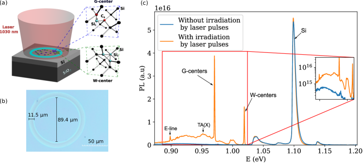
- Femtosecond laser pulses (1030 nm, <200 fs, 1 kHz repetition rate) were focused onto SOI wafers using a 750 mm plano-convex lens to induce localized thermal annealing.
- Samples were irradiated with 1–5 pulses at energies of 95–218 µJ, creating defects in the 220 nm top Si layer.
- Two types of SOI substrates were used: one implanted with 12C+ ions at 34 keV and doses of 1×10¹² and 1×10¹³ cm⁻², and pristine SOI with residual carbon.
- Post-irradiation annealing at 125 °C for 5 minutes was applied to study defect evolution and selective G-center erasure.
- Photoluminescence (PL) measurements were performed at 12 K using a 405 nm CW pump laser and a spectrometer with an InGaAs detector (900–1600 nm).
- Time-resolved PL and temperature-dependent PL were used to analyze radiative lifetimes, zero-phonon line (ZPL) broadening, and thermal redshift of ZPLs.
Experimental results
Research questions
- RQ1Can femtosecond laser annealing be used to create W- and G-centers in SOI substrates with optical properties comparable to those from standard implantation methods?
- RQ2Is carbon ion implantation necessary for the formation of G- and W-centers in SOI via this laser-based method?
- RQ3Can low-temperature annealing selectively erase G-centers while enhancing W-center emission?
- RQ4Can the laser process enable deterministic, on-demand, and spatially confined creation of quantum emitters in silicon?
Key findings
- The photoluminescence radiative lifetime, ZPL broadening, and temperature-dependent ZPL shift of W- and G-centers created by femtosecond laser annealing are comparable to those reported in the literature for conventionally fabricated defects.
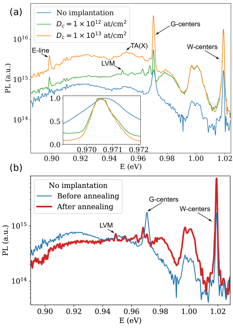
- G- and W-centers were successfully created in pristine SOI substrates without any carbon implantation, indicating that residual carbon in the wafer is sufficient for defect formation.
- The ZPL of G-centers in non-implanted samples showed broader lines and a blue shift compared to implanted samples, consistent with lower internal strain and lower defect density.
- Low-temperature annealing (125 °C, 5 min) selectively erased G-centers while slightly enhancing the PL emission intensity of W-centers, contrary to expectations based on prior studies.
- The spatial confinement of defect creation matched the laser spot size (~178 µm waist), enabling localized and potentially single-defect engineering.
- The method enables deterministic, on-demand, and area-restricted creation of W-centers without ion implantation, offering a scalable and cost-effective alternative for quantum photonic integration.
Better researchstarts right now
From reading papers to final review, dramatically reduce your research time.
No credit card · Free plan available
This review was created by AI and reviewed by human editors.