[论文解读] 3D photonics for ultra-low energy, high bandwidth-density chip data links
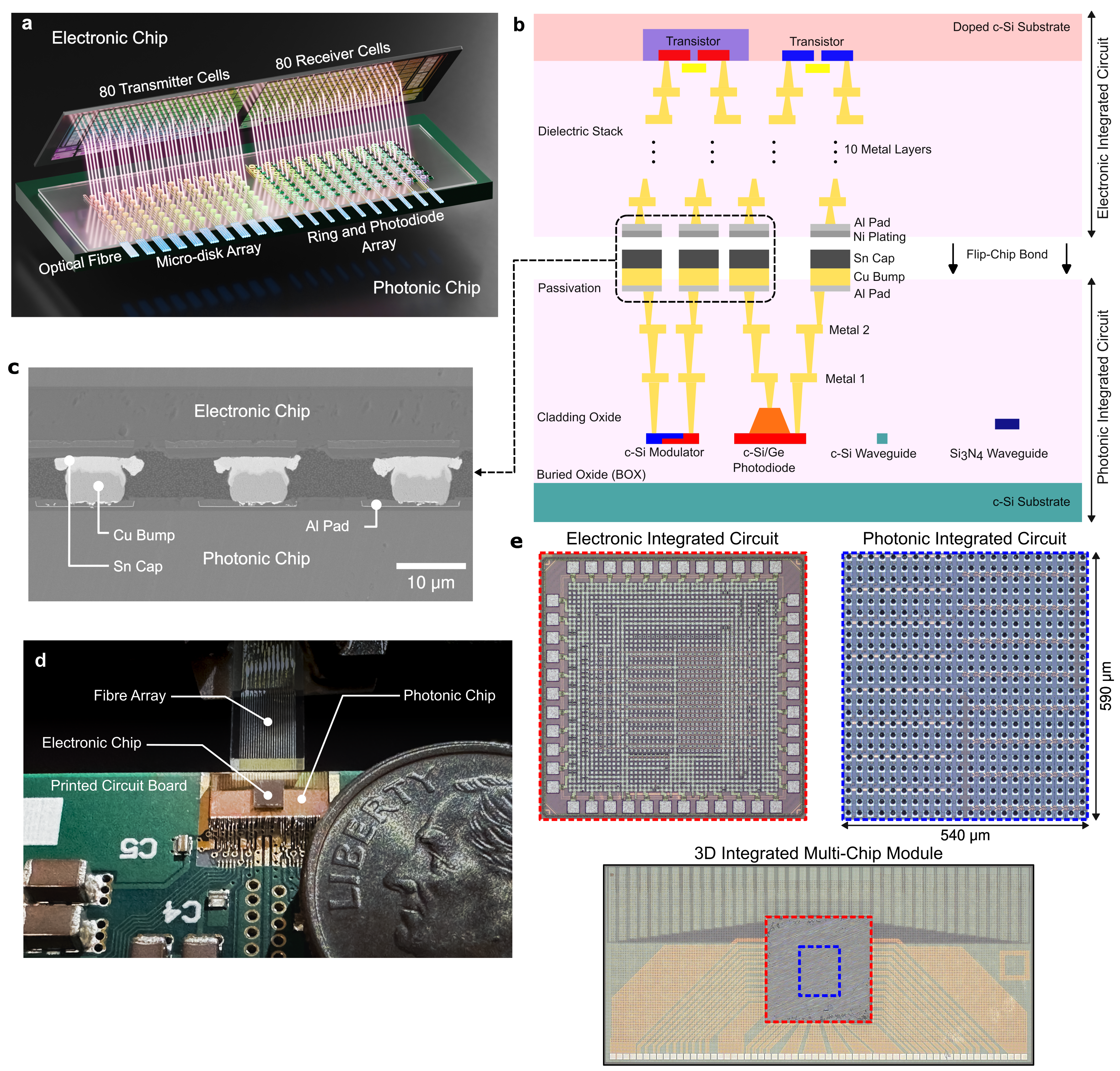
展示一个3D集成光电子收发器,80个发射通道和80个接收通道,总带宽达到800 Gb/s,带宽密度达到5.3 Tb/s/mm^2,耗能约为120 fJ/比特,利用低电容3D键合和CMOS光子集成共同设计。
Artificial intelligence (AI) hardware is positioned to unlock revolutionary computational abilities across diverse fields ranging from fundamental science [1] to medicine [2] and environmental science [3] by leveraging advanced semiconductor chips interconnected in vast distributed networks. However, AI chip development has far outpaced that of the networks that connect them, as chip computation speeds have accelerated a thousandfold faster than communication bandwidth over the last two decades [4, 5]. This gap is the largest barrier for scaling AI performance [6, 7] and results from the disproportionately high energy expended to transmit data [8], which is two orders of magnitude more intensive than computing [9]. Here, we show a leveling of this long-standing discrepancy and achieve the lowest energy optical data link to date through dense 3D integration of photonic and electronic chips. At 120 fJ of consumed energy per communicated bit and 5.3 Tb/s bandwidth per square millimeter of chip area, our platform simultaneously achieves a twofold improvement in both energy consumption and bandwidth density relative to prior demonstrations [10, 11]. These improvements are realized through employing massively parallel 80 channel microresonator-based transmitter and receiver arrays operating at 10 Gb/s per channel, occupying a combined chip footprint of only 0.32 mm2. Furthermore, commercial complementary metal-oxide-semiconductor (CMOS) foundries fabricate both the electronic and photonic chips on 300 mm wafers, providing a clear avenue to volume scaling. Through these demonstrated ultra-energy efficient, high bandwidth data communication links, this work eliminates the bandwidth bottleneck between spatially distanced compute nodes and will enable a fundamentally new scale of future AI computing hardware without constraints on data locality.
研究动机与目标
- 通过缩小芯片计算速度与互连带宽之间的差距,解决AI硬件的数据传输瓶颈。
- 在3D堆叠中演示密集集成的光子和电子芯片实现的高带宽、能效较高的芯片间通信。
- 在尽量降低每通道能耗的前提下扩展数据通道数,以实现实用且体积可扩展的光子链路。
- 展示在300 mm晶圆上用CMOS制造的光电子收发器在大规模部署中的可行性。
提出的方法
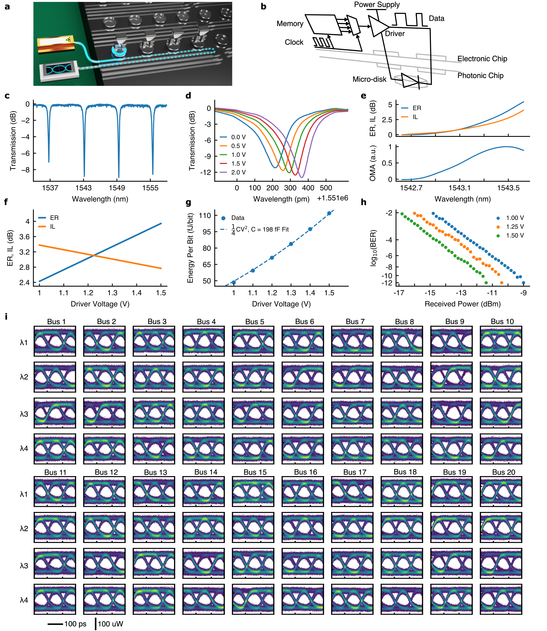
- 开发一个3D集成收发器,80个发射单元和80个接收单元,分成20条波导总线,每总线4个波长。
- 使用间距15 μm的铜柱焊球、直径10 μm的焊球(总距25 μm)实现光子芯片与电子芯片之间的高密度绑定。
- 协同设计低电容光子器件与CMOS驱动器,使发射端总电容约200 fF、接收端能量约70 fJ/比特。
- 在80个通道上每通道10 Gb/s工作,以实现总计800 Gb/s,晶片面积为0.32 mm^2(发射端)和阵列总面积0.15 mm^2/0.32 mm^2(发射端/阵列)。
- 使用Miller 1/4 CV^2模型对每比特能耗进行表征,并测量发射端与接收端性能的每通道能耗。
- 演示一个完整的发射端到接收端光学数据链路,跨越两个独立收发器,具备四通道波长,在特定光功率条件下BER达到10^-12量级以下。
实验结果
研究问题
- RQ1在芯片尺度下,密集集成的3D光电子收发器的每比特能耗和带宽密度可达到何种水平?
- RQ2高通道数(80x80)收发器是否可以在保持高总数据速率的同时实现低每通道能耗?
- RQ3哪些键合和器件设计选择能在不影响可靠性或BER的前提下最大化通道密度?
- RQ4在完整的发射端到接收端链路中,集成3D光电子链路的实际BER性能与灵敏度如何?
主要发现
- 80通道发射阵列与80通道接收阵列在0.32 mm^2(发射端)面积内实现总计800 Gb/s,带宽密度为5.3 Tb/s/mm^2。
- 发射端全链路能耗为120 fJ/比特,接收端在10 Gb/s工作时为70 fJ/比特,发射端到接收端的总体链路能耗约为120 fJ/比特。
- 电容预算(焊盘、焊球、微圆盘、光二极管和驱动器)约为199 fF的发射端电容,与测量得到的每比特能耗一致。
- 使用四通道的完整发射端到接收端光学链路在测试条件下BER≤6×10^-8,且各通道的开眼图正常。
- 采用15 μm间距、10 μm焊球直径(25 μmpitch)的键合实现了稳健的2.1 kg晶粒对晶粒键合和较低的寄生效应,支持高密度集成。
- 该数据链路在四通道激光器和四波长情况下工作,在有利条件下BER接近10^-12。
更好的研究,从现在开始
从论文设计到论文写作,大幅缩短您的研究时间。
无需绑定信用卡
本解读由 AI 生成,并经人工编辑审核。