
[论文解读] A superconducting-nanowire single-photon camera with 400,000 pixels
本论文提出了一种基于热耦合行-列复用架构的400,000像素超导纳米线单光子相机,采用交错排列的WSi纳米线。该器件实现了5×5 µm像素分辨率,在370 nm和635 nm波长下量子效率达到1,暗计数率为0.13 cps(全阵列),在0.8 K下运行,并通过四条微波同轴线实现可扩展读出。
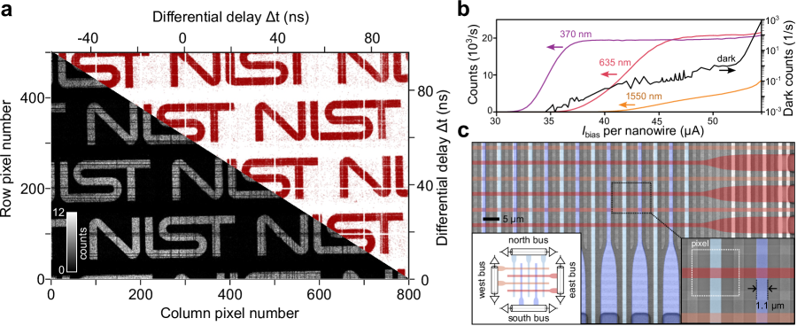
For the last 50 years, superconducting detectors have offered exceptional sensitivity and speed for detecting faint electromagnetic signals in a wide range of applications. These detectors operate at very low temperatures and generate a minimum of excess noise, making them ideal for testing the non-local nature of reality, investigating dark matter, mapping the early universe, and performing quantum computation and communication. Despite their appealing properties, however, there are currently no large-scale superconducting cameras - even the largest demonstrations have never exceeded 20 thousand pixels. This is especially true for one of the most promising detector technologies, the superconducting nanowire single-photon detector (SNSPD). These detectors have been demonstrated with system detection efficiencies of 98.0%, sub-3-ps timing jitter, sensitivity from the ultraviolet (250nm) to the mid-infrared (10um), and dark count rates below 6.2e-6 counts per second (cps), but despite more than two decades of development they have never achieved an array size larger than a kilopixel. Here, we report on the implementation and characterization of a 400,000 pixel SNSPD camera, a factor of 400 improvement over the previous state-of-the-art. The array spanned an area 4x2.5 mm with a 5x5um resolution, reached unity quantum efficiency at wavelengths of 370 nm and 635 nm, counted at a rate of 1.1e5 cps, and had a dark count rate of 1e-4 cps per detector (corresponding to 0.13 cps over the whole array). The imaging area contains no ancillary circuitry and the architecture is scalable well beyond the current demonstration, paving the way for large-format superconducting cameras with 100% fill factors and near-unity detection efficiencies across a vast range of the electromagnetic spectrum.
研究动机与目标
- 通过实现大格式、高密度像素阵列,克服超导纳米线单光子探测器(SNSPD)的可扩展性限制。
- 解决SNSPD多路复用的挑战,因为SNSPD产生低幅度、超宽带脉冲,难以在大规模下高效读出。
- 开发一种可扩展的低噪声读出架构,保持高信噪比,并在千像素及以上阵列中最小化串扰。
- 在大尺寸成像区域上实现接近单位的量子效率和极低的暗计数率,填充因子达100%。
- 展示一种实用且可重复的大规模SNSPD阵列制造工艺,采用标准光刻技术和热耦合原理。
提出的方法
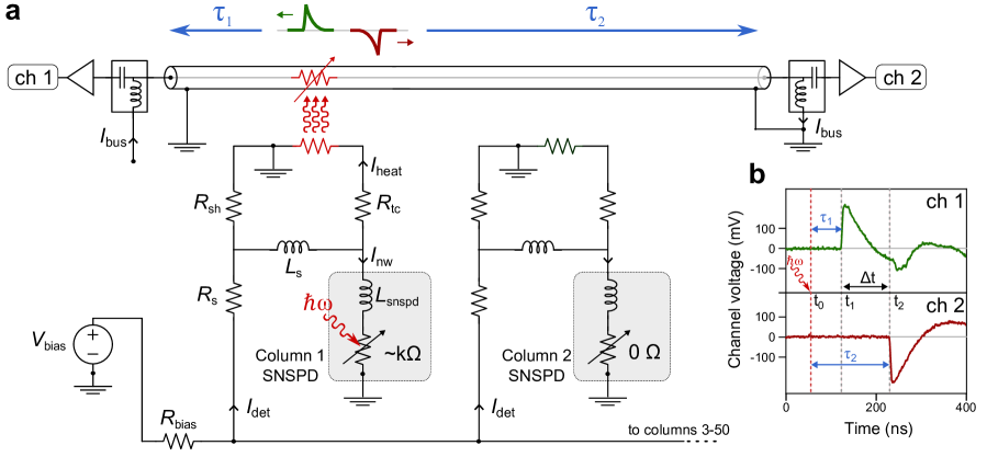
- 采用热耦合行-列复用架构,其中SNSPD以网格形式排列,并通过电阻热耦合器连接到共享读出总线。
- 使用4 nm厚的WSi薄膜制成交错排列的行和列纳米线探测器,Tc = 3.4 K,面内电感为250 pH/sq,线宽1.1 µm,间距5 µm。
- 实施四总线读出系统,使用8条微波同轴线,每条总线通过热耦合器连接50个探测器,实现多路复用。
- 优化电路参数(R_bias = 1000 Ω,R_s = 80 Ω,R_sh = 16 Ω,R_tc = 16 Ω,L_s = 1.25 µH,L_snspd = 1.14 µH),以确保电流分布均匀、串扰低且复位时间快。
- 采用步进光刻技术将10个探测器的单元结构复制到1000×1000阵列中,实现均匀良率的可扩展制造。
- 对总线的时间延迟数据进行时间标记和直方图分析,以重建二维图像并量化探测性能。
实验结果
研究问题
- RQ1能否通过热耦合与多路复用技术,为大格式SNSPD阵列开发一种可扩展且低串扰的读出架构?
- RQ2在保持高量子效率和低暗计数率的前提下,超导纳米线单光子相机的最大可实现像素数是多少?
- RQ3与以往多路复用方案相比,该热耦合行-列架构在信噪比和可扩展性方面表现如何?
- RQ4在使用标准光刻技术时,大尺度SNSPD阵列的制造良率和均匀性能在多大程度上保持?
- RQ5400,000像素的SNSPD阵列能否同时实现接近单位的量子效率和亚cps量级的暗计数率?
主要发现
- SNSPD阵列实现了400,000像素,像素分辨率为5×5 µm,相比先前最先进的1,024像素提升了400倍。
- 该阵列在370 nm和635 nm波长下表现出单位量子效率,表明在可见光波段实现了近乎完美的光子探测。
- 暗计数率测量为每探测器1.0×10⁻⁴ cps,全阵列总计0.13 cps,证实了低噪声运行。
- 系统在0.8 K下运行,计数率达1.1×10⁵ cps,表明具有高动态范围和快速复位能力。
- 读出架构仅使用四条微波同轴线即可覆盖整个阵列,实现了可扩展、低热负载的多路复用,且串扰极小。
- 所制造的阵列在成像区域无辅助电路,填充因子达100%,并展示了向更大格式扩展的完全可扩展性。
更好的研究,从现在开始
从阅读论文到最终审阅,大幅缩短您的研究时间。
无需绑定信用卡
本解读由 AI 生成,并经人工编辑审核。