
[论文解读] A Unified Cryptoprocessor for Lattice-based Signature and Key-exchange
本文提出了一种统一、紧凑且可编程的格基后量子密码学专用处理器架构,集成CRYSTALS-Dilithium(数字签名)与Saber(密钥封装机制)。通过利用共享的算法组件——尤其是基于NTT的统一多项式乘法器和可重构的Keccak核心——该设计在极小的面积开销下实现了高性能,FPGA上运行频率达200 MHz,且在两种方案中关键操作的执行时间均低于100 μs。
We propose design methodologies for building a compact, unified and programmable cryptoprocessor architecture that computes post-quantum key agreement and digital signature. Synergies in the two types of cryptographic primitives are used to make the cryptoprocessor compact. As a case study, the cryptoprocessor architecture has been optimized targeting the signature scheme 'CRYSTALS-Dilithium' and the key encapsulation mechanism (KEM) 'Saber', both finalists in the NIST's post-quantum cryptography standardization project. The programmable cryptoprocessor executes key generations, encapsulations, decapsulations, signature generations, and signature verifications for all the security levels of Dilithium and Saber. On a Xilinx Ultrascale+ FPGA, the proposed cryptoprocessor consumes 18,406 LUTs, 9,323 FFs, 4 DSPs, and 24 BRAMs. It achieves 200 MHz clock frequency and finishes CCA-secure key-generation/encapsulation/decapsulation operations for LightSaber in 29.6/40.4/58.3$μ$s; for Saber in 54.9/69.7/94.9$μ$s; and for FireSaber in 87.6/108.0/139.4$μ$s, respectively. It finishes key-generation/sign/verify operations for Dilithium-2 in 70.9/151.6/75.2$μ$s; for Dilithium-3 in 114.7/237/127.6$μ$s; and for Dilithium-5 in 194.2/342.1/228.9$μ$s, respectively, for the best-case scenario. On UMC 65nm library for ASIC the latency is improved by a factor of two due to a 2x increase in clock frequency.
研究动机与目标
- 设计一种紧凑、统一且可编程的密码处理器,支持后量子密钥封装(Saber)与数字签名(Dilithium)方案。
- 利用NTT友好(Dilithium)与NTT不友好(Saber)格基方案之间的算法与结构协同效应,最小化硬件开销。
- 实现在资源受限环境(如支持TLS的系统)中实际部署所需的高性能与低面积消耗。
- 通过模块化指令集架构,支持未来格基方案(如CRYSTALS-Kyber)的可扩展性。
- 通过为共享组件集成掩码策略,为安全、抗侧信道攻击的实现提供基础。
提出的方法
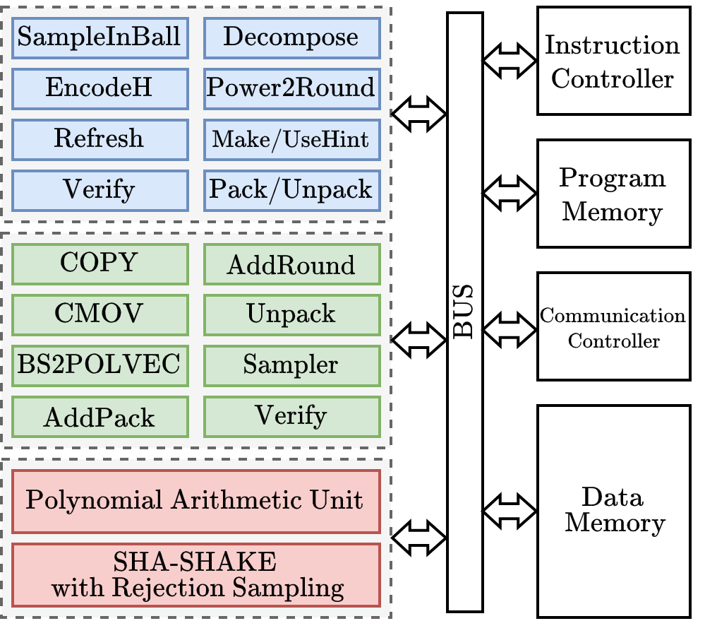
- 设计一种统一的指令集架构,通过共享硬件单元支持Dilithium与Saber的操作。
- 实现一个单一的基于NTT的多项式乘法器,通过特殊素数模数支持NTT友好(Dilithium)与优化后的NTT不友好(Saber)算术。
- 开发一个可重构的Keccak核心封装,高效处理SHA3与SHAKE操作所需的运行时输入预处理与输出后处理,这些操作在两种方案中均被使用。
- 通过流水线数据通路与缓冲策略优化内存访问模式,减少冗余读写周期。
- 集成一个双模式算术单元,用于多项式乘法与模约减,共享两种方案的逻辑。
- 采用软硬件协同设计方法,支持运行时重构与多种安全等级。
![Figure 1: Distribution of a coefficient after a multiplication between a secret and a public polynomial. The secret and public coefficients are in the range $[-\frac{\mu}{2},\frac{\mu}{2}]$ and $[0,q-1]$ , respectively.](https://ar5iv.labs.arxiv.org/html/2210.07412/assets/images/plot_NTT_error.png)
实验结果
研究问题
- RQ1尽管算法结构不同,单个密码处理器能否高效且紧凑地支持格基密钥封装(Saber)与数字签名(Dilithium)方案?
- RQ2NTT友好与NTT不友好格基方案之间存在哪些可利用的架构协同效应,以最小化面积开销?
- RQ3统一硬件设计在保持关键操作(如密钥生成与签名验证)高吞吐量的同时,如何减少资源消耗?
- RQ4共享构建模块(如NTT与Keccak核心)在不同后量子方案中可重用的程度如何,同时不牺牲性能?
- RQ5所提出的密码处理器能否通过极少修改扩展支持其他格基方案(如CRYSTALS-Kyber)?
主要发现
- 该密码处理器在Xilinx Ultrascale+ FPGA上实现200 MHz时钟频率,功耗为18,406 LUTs、9,323 FFs、4 DSPs与24 BRAMs。
- 对于LightSaber,密钥生成、封装与解封装分别耗时29.6、40.4与58.3 μs。
- 对于Saber,相同操作分别耗时54.9、69.7与94.9 μs,而Dilithium-3签名与验证在最佳情况下分别耗时237与127.6 μs。
- 在65nm ASIC上,由于时钟频率提升2倍,性能提升一倍,Saber操作的估计延迟分别为27.5、34.9与47.5 μs。
- 统一的NTT乘法器相比仅支持Dilithium的设计显著降低了面积开销,尤其通过利用特殊素数模数优化Saber的NTT计算。
- 优化后的Keccak封装减少了不必要的内存访问,提升了哈希操作的吞吐量并降低了功耗。
更好的研究,从现在开始
从阅读论文到最终审阅,大幅缩短您的研究时间。
无需绑定信用卡
本解读由 AI 生成,并经人工编辑审核。