[论文解读] Exciton states in monolayer MoSe2 and MoTe2 probed by upconversion spectroscopy
本研究利用六方氮化硼(hBN)封装的单层MoSe2和MoTe2中的上转换光谱学,解析了此前难以观测的激发态激子态,实现了低于1.5 meV的线宽。作者识别出一种共振的激子-激子爱格尔散射机制作为上转换的起源,实现了对基态以上200 meV以内的激子态的偏压可调谐观测,通过反射率和光致发光激发光谱学获得直接证实。
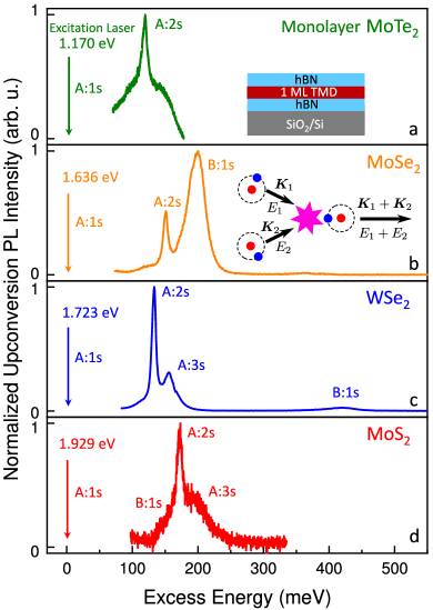
Transitions metal dichalcogenides (TMDs) are direct semiconductors in the atomic monolayer (ML) limit with fascinating optical and spin-valley properties. The strong optical absorption of up to 20 % for a single ML is governed by excitons, electron-hole pairs bound by Coulomb attraction. Excited exciton states in MoSe$_2$ and MoTe$_2$ monolayers have so far been elusive due to their low oscillator strength and strong inhomogeneous broadening. Here we show that encapsulation in hexagonal boron nitride results in emission line width of the A:1$s$ exciton below 1.5 meV and 3 meV in our MoSe$_2$ and MoTe$_2$ monolayer samples, respectively. This allows us to investigate the excited exciton states by photoluminescence upconversion spectroscopy for both monolayer materials. The excitation laser is tuned into resonance with the A:1$s$ transition and we observe emission of excited exciton states up to 200 meV above the laser energy. We demonstrate bias control of the efficiency of this non-linear optical process. At the origin of upconversion our model calculations suggest an exciton-exciton (Auger) scattering mechanism specific to TMD MLs involving an excited conduction band thus generating high energy excitons with small wave-vectors. The optical transitions are further investigated by white light reflectivity, photoluminescence excitation and resonant Raman scattering confirming their origin as excited excitonic states in monolayer thin semiconductors.
研究动机与目标
- 解析在传统测量中因非均匀展宽和振子强度低而被掩盖的单层MoSe2和MoTe2中长期难以观测的激发态激子态。
- 证明六方氮化硼(hBN)封装显著减小了激子线宽,从而实现了对激发态的高分辨率光谱学表征。
- 识别过渡金属二硫属化物单层中上转换现象背后的微观机制,特别是激子-激子散射的作用。
- 建立一种非线性光学技术——上转换光谱学,用于探测完整的激子能级谱,包括基态以上的态。
- 通过白光反射率和光致发光激发(PLE)光谱学等互补技术,验证上转换信号的起源。
提出的方法
- 采用可调谐的钛蓝宝石激光器,对准hBN封装的单层MoSe2和MoTe2中A:1s激子跃迁,实施共振光致发光上转换光谱学。
- 通过hBN封装,实现低于1.5 meV的线宽(MoSe2中为1.5 meV,MoTe2中为3 meV),从而解析出精细的激子特征。
- 利用白光反射率和光致发光激发(PLE)光谱学,独立确认上转换发射峰的能量位置。
- 基于包含导带激发的激子-激子爱格尔散射,构建了理论模型,矩阵元由有效质量和k·p理论推导得出。
- 采用多体方法计算爱格尔复合速率,综合考虑能量守恒、动量分布和交换相互作用。
- 将上转换过程建模为一种共振的双激子散射事件,其中一个激子湮灭,并将能量和动量转移,生成高能量、小波矢的激子。
实验结果
研究问题
- RQ1在共振激发的单层MoSe2和MoTe2中观测到的上转换发射是由什么引起的?其基本物理机制是什么?
- RQ2为什么MoSe2和MoTe2中的激发态激子态在标准光致发光测量中难以观测,又如何实现其探测?
- RQ3hBN封装如何实现对这些二维半导体中此前未解析的激子态的观测?
- RQ4通过外部电场栅压,上转换过程的效率在多大程度上可被调控?
- RQ5库仑相互作用和能带结构在实现单层TMD中高效激子-激子散射中起到何种作用?
主要发现
- hBN封装将A:1s激子的线宽减小至MoSe2中低于1.5 meV,MoTe2中低于3 meV,从而实现了高分辨率光谱学。
- 上转换光谱学揭示了激发能以上高达200 meV的激发态激子态,证实了两种材料中A:2s和B:1s态的存在。
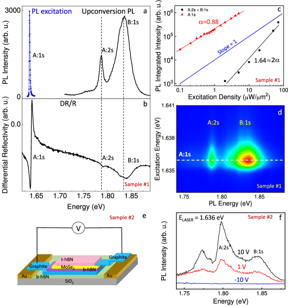
- 上转换过程可通过外加栅压高效调控,表明非线性光学响应具有可调谐性。
- 上转换的起源被确定为一种涉及激发导带的共振激子-激子爱格尔散射过程,该过程高效生成高能量、小动量的激子。
- 理论建模证实,强库仑相互作用和与激发能带的共振耦合增强了爱格尔散射速率,使其主导于其他弛豫路径。
- 在典型条件下(T = 4 K,nX = 10^9 cm⁻²),测得的爱格尔复合时间约为~25 ps,与观测到的上转换效率一致。
更好的研究,从现在开始
从论文设计到论文写作,大幅缩短您的研究时间。
无需绑定信用卡
本解读由 AI 生成,并经人工编辑审核。