
[论文解读] Imaging the breaking of electrostatic dams in graphene for ballistic and viscous fluids
本研究利用扫描隧道势谱学(STP)在纳米尺度分辨率下成像石墨烯中的准粒子输运,揭示了非欧姆输运剖面以及窄通道中的超弹道导电性。结果表明,在77 K时,粘性电子流超过弹道极限,测得的电子-电子散射长度约为100 nm,运动粘度约为2.5×10³ cm²/s,证实了石墨烯费米液体中的流体行为。
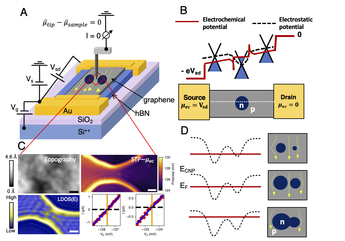
The flow of charge carriers in materials can, under some circumstances, mimic the flow of viscous fluids. In order to visualize the consequences of such effects, new methodologies must be developed that can probe the quasiparticle flow profile with nm-scale resolution as the geometric parameters of the system are continuously evolved. In this work, scanning tunneling potentiometry (STP) is used to image quasiparticle flow around engineered electrostatic barriers in graphene/hBN heterostructures. Measurements are performed as electrostatic dams - defined by lateral pn-junction barriers - are broken within the graphene sheet, and carriers move through conduction channels with physical widths that vary continuously from pinch-off to um-scale. Local, STP measurements of the electrochemical potential allow for direct characterization of the evolving flow profile, which we compare to finite-element simulations of a Stokesian fluid with varying parameters. Our results reveal distinctly non-Ohmic flow profiles, with charge dipoles forming across barriers due to carrier scattering and accumulation on the upstream side, and depletion downstream. Conductance measurements of individual channels, meanwhile, reveal that at low temperatures the quasiparticle flow is ballistic, but as the temperature is raised there is a Knudsen-to-Gurzhi regime crossover where the fluid becomes viscous and the channel conductance exceeds the ballistic limit set by Sharvin conductance. These results provide a clear illustration of how carrier flow in a Fermi fluid evolves as a function of carrier density, channel width, and temperature. They also demonstrate how STP can be used to extract key parameters of quasiparticle transport, with a spatial resolution that exceeds that of other methods by orders of magnitude.
研究动机与目标
- 通过连续调节几何参数(如通道宽度),在纳米尺度空间分辨率下可视化石墨烯中准粒子流的分布。
- 通过改变温度和载流子浓度,探测石墨烯中从弹道输运到粘性电子流的转变过程。
- 证明扫描隧道势谱学(STP)能够以优于其他方法的分辨率,直接测量电化学势分布。
- 从实验STP数据中提取关键流体动力学参数,如电子-电子散射长度和运动粘度。
- 将观测到的流型与斯托克斯流体模型的有限元模拟结果进行对比验证。
提出的方法
- 利用扫描隧道势谱学(STP)在亚100 nm空间分辨率下测绘石墨烯表面的局域电化学势。
- 通过STM针尖施加电压脉冲,在石墨烯中现场构建静电势垒(p-n结),形成可调的狭窄通道和“静电坝”。
- 该方法可实现通道宽度从微米量级到完全夹断的连续调节,从而实现实时观测流型的演化过程。
- 采用斯托克斯流体的有限元模拟方法,对不同参数下的实验流型进行建模并与之比较。
- 基于托马斯-费米近似,通过自洽求解耦合方程组,对圆形p-n结中的电荷密度和电势分布进行理论建模。
- 分析石墨烯p-n结中的非线性屏蔽效应,以评估在不同长度尺度下流体动力学建模的有效性。
实验结果
研究问题
- RQ1当静电坝被破坏且通道宽度连续变化时,石墨烯中准粒子流的分布如何演化?
- RQ2在不同温度下,局域电化学势测量中,粘性输运与弹道输运分别呈现何种特征?
- RQ3STP在多大程度上能够分辨石墨烯中诸如电荷偶极子和超弹道导电性等流体动力学特征?
- RQ4石墨烯中电子-电子散射长度和运动粘度与理论预测及已有实验观测结果相比如何?
- RQ5斯托克斯流体的有限元模拟能否定量再现STP实测的电势分布?
主要发现
- 在4.5 K时,准粒子流为弹道输运,通道电导达到Sharvin电导极限,表明散射极小。
- 在77 K时,通道电导超过弹道极限,表现出与粘性流一致的超弹道行为。
- 在77 K时测得的电子-电子散射长度约为100 nm,表明存在强烈的多体相互作用。
- 电子液体的运动粘度估计值约为2.5×10³ cm²/s,证实了粘性流体输运行为。
- 由于上游载流子积累和下游耗尽,势垒两侧形成电荷偶极子,这是非欧姆输运的典型特征。
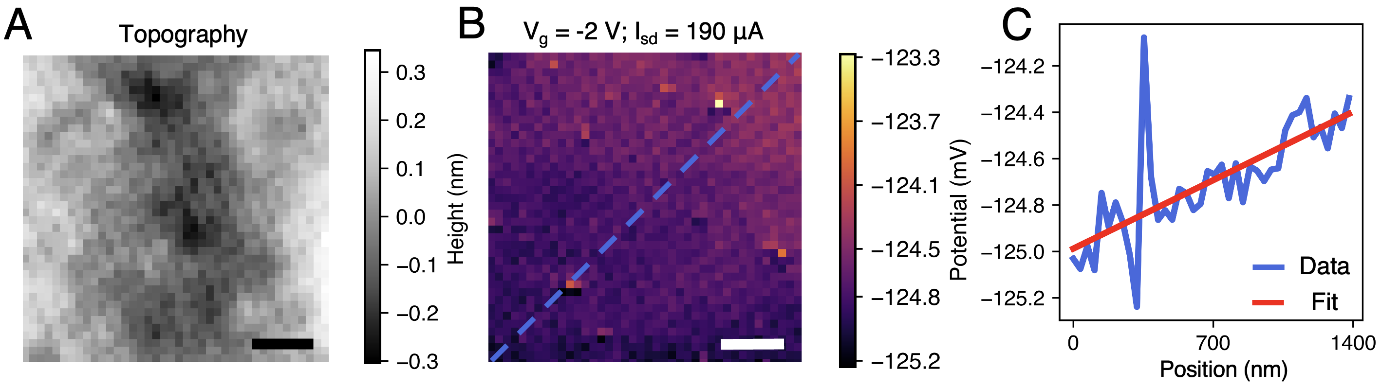
- STP测量实现了纳米尺度空间分辨率的电势梯度分辨,其分辨率较其他扫描探针技术高出一个量级以上。
更好的研究,从现在开始
从阅读论文到最终审阅,大幅缩短您的研究时间。
无需绑定信用卡
本解读由 AI 生成,并经人工编辑审核。