
[论文解读] On-chip quantum interference between independent lithium niobate-on-insulator photon-pair sources
该论文展示了基于周期极化绝缘衬底上铌酸锂(LNOI)波导的两个独立光子对源之间在芯片上的量子干涉。通过将可编程马赫-曾德尔干涉仪与高亮度自发参量下转换(SPDC)源集成,作者实现了96.8(3.6)%的可见度量子干涉,实现了可扩展、芯片集成的量子光子电路,具备高不可区分性和高亮度。
Generating and interfering non-classical states of light is fundamental to optical quantum information science and technology. Quantum photonic integrated circuits provide one pathway towards scalability by combining nonlinear sources of non-classical light and programmable circuits in centimeter-scale devices. The key requirements for quantum applications include efficient generation of indistinguishable photon-pairs and high-visibility programmable quantum interference. Here, we demonstrate a lithium niobate-on-insulator (LNOI) integrated photonic circuit that generates a two-photon path-entangled state, and a programmable interferometer for quantum interference. We generate entangled photons with $\sim2.3 imes10^8$ pairs/s/mW brightness and perform quantum interference experiments on the chip with $96.8\pm3.6\%$ visibility. LNOI is an emerging photonics technology that has revolutionized high-speed modulators and efficient frequency conversion. Our results provide a path towards large-scale integrated quantum photonics including efficient photon-pair generation and programmable circuits for applications such as boson sampling and quantum communications.
研究动机与目标
- 通过结合高亮度光子对生成与可编程量子干涉,实现可扩展的芯片集成量子光子电路。
- 通过利用绝缘衬底上铌酸锂(LNOI)的强非线性和电光特性,克服硅和氮化硅平台的局限性。
- 通过芯片内干涉实现独立生成光子之间的高可见度量子干涉,这是玻色采样和量子通信中实现量子优势的关键要求。
- 证明LNOI技术可在单一集成平台上同时支持高效的光子对生成与高保真度量子干涉。
提出的方法
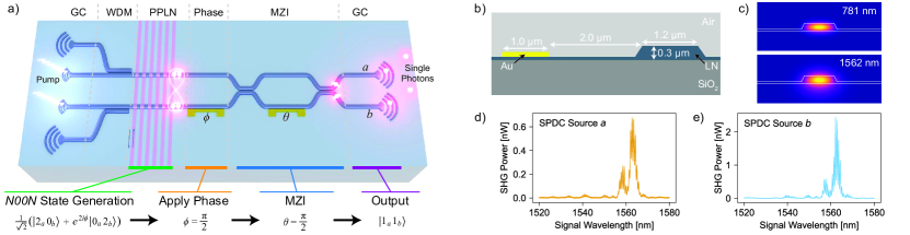
- 芯片集成了两个相同的周期极化LNOI波导,用于自发参量下转换(SPDC),生成路径 entangled 的N00N态。
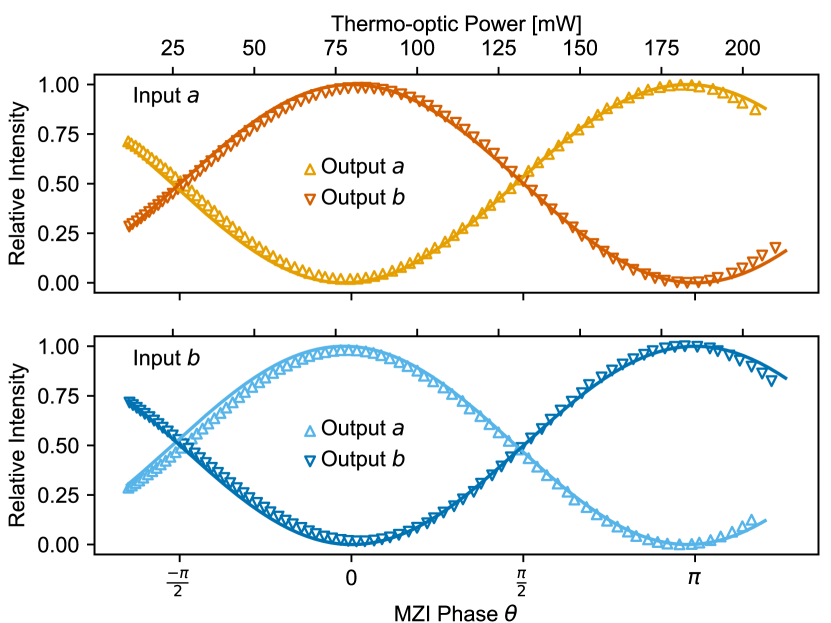
- 具有热光相位延迟器的马赫-曾德尔干涉仪(MZI)可实现对两个输出模式间量子干涉的可调谐控制。
- 光子对生成由波长为781 nm的泵浦激光驱动,通过II型相位匹配在1562 nm波长处产生相关光子对。
- 芯片内亮度测量值约为~2.3×10⁸对/秒/mW,显著高于典型体材料SPDC源。
- 通过受控的N00N态相位扫描与MZI调节,量化量子干涉可见度,输出态由单光子探测器测量。
- 离芯片的洪欧曼德尔(HOM)实验验证了光子不可区分性,测得可见度为83.2±0.1%, dip宽度为71.9(0.5) fs。
实验结果
研究问题
- RQ1基于LNOI的独立芯片光子对源能否实现高可见度量子干涉?
- RQ2周期极化LNOI波导中SPDC源的芯片内亮度是多少?
- RQ3单个LNOI芯片能否同时集成高效光子对生成与可编程干涉仪以实现量子干涉?
- RQ4芯片内量子干涉的可见度与离芯片HOM测量中光子不可区分性的可见度相比如何?
- RQ5LNOI技术在多大程度上能够实现可扩展的、集成化的量子光子电路,以实现近期量子优势?
主要发现
- 芯片在独立生成光子之间的芯片内量子干涉中实现了96.8(3.6)%的可见度,证明了高不可区分性。
- 芯片内光子对亮度达到~2.3×10⁸对/秒/mW,超过典型自由空间SPDC源,包括基于ppKTP的源。
- 洪欧曼德尔实验确认了光子不可区分性,可见度为83.2±0.1%,受限于光纤分束器带宽。
- 光纤耦合后光子的光谱带宽估计约为50 nm,与71.9(0.5) fs的HOM dip宽度一致。
- 与芯片内干涉相比,观测到的可见度降低,归因于带宽受限和离芯片组件的对准误差。
- SPDC源与可编程干涉仪在单个LNOI芯片上的集成,为玻色采样和量子计量等量子信息任务提供了一个可扩展的平台。
更好的研究,从现在开始
从阅读论文到最终审阅,大幅缩短您的研究时间。
无需绑定信用卡
本解读由 AI 生成,并经人工编辑审核。