
[论文解读] Tunable quantum emitters on large-scale foundry silicon photonics
该论文提出了一种混合集成平台,将InAs/InP量子点微芯片与大规模300 mm代工厂硅光子学相结合,通过非易失性斯塔克移位实现电控可调的单光子发射。该系统实现了单个发射器的可寻址性、共振荧光以及亚3 dB的光纤耦合,为在商业半导体代工厂中实现可编程、片上量子处理器铺平了道路。
Controlling large-scale many-body quantum systems at the level of single photons and single atomic systems is a central goal in quantum information science and technology. Intensive research and development has propelled foundry-based silicon-on-insulator photonic integrated circuits to a leading platform for large-scale optical control with individual mode programmability. However, integrating atomic quantum systems with single-emitter tunability remains an open challenge. Here, we overcome this barrier through the hybrid integration of multiple InAs/InP microchiplets containing high-brightness infrared semiconductor quantum dot single photon emitters into advanced silicon-on-insulator photonic integrated circuits fabricated in a 300~mm foundry process. With this platform, we achieve single photon emission via resonance fluorescence and scalable emission wavelength tunability through an electrically controlled non-volatile memory. The combined control of photonic and quantum systems opens the door to programmable quantum information processors manufactured in leading semiconductor foundries.
研究动机与目标
- 解决将可调谐、单光子发射器与大规模光子集成电路(PICs)集成以实现可扩展量子信息处理的挑战。
- 通过利用代工厂硅基绝缘体(SOI)PICs的可扩展性与低损耗特性,克服传统III-V族单片集成PICs的高传播损耗与缺乏单个发射器控制的局限。
- 通过与转移印刷的InP芯片集成及非易失性电控调谐,实现对多个量子点发射器的独立控制。
- 通过SOI PIC中优异的泵浦抑制,实现高保真度单光子发射与共振荧光,同时背景噪声极低。
- 开发一种与商业半导体代工厂兼容的可扩展、可制造平台,为未来大规模量子光子系统铺平道路。
提出的方法
- 采用300 mm代工厂工艺制造先进的SOI光子集成电路(PICs),通过迭代设计与后处理技术实现亚3 dB的光纤耦合效率。
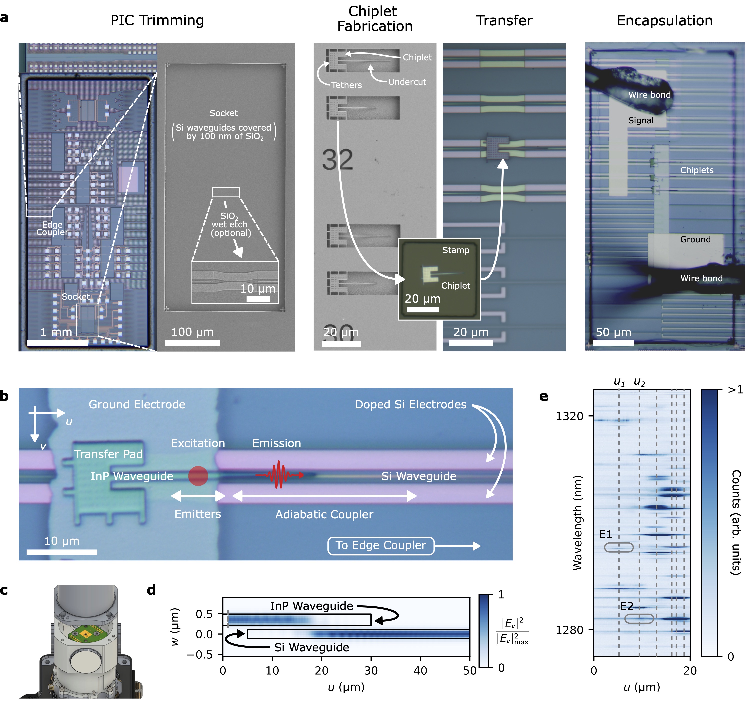
- 采用可扩展、对准精确的转移印刷方法,将包含高亮度InAs/InP量子点的多个InAs/InP微芯片转移到SOI PIC上。
- 通过聚焦激光束实现共振激发,以获得来自单个量子点的高信噪比共振荧光。
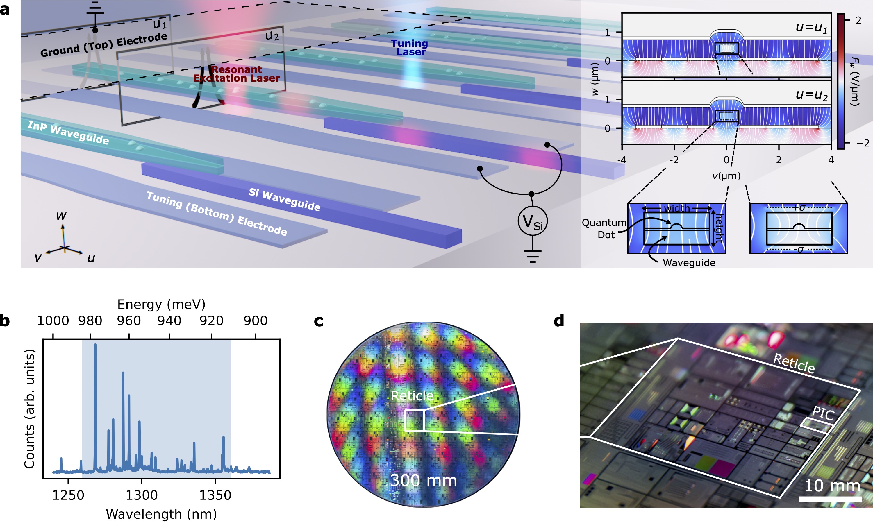
- 在每个量子点附近集成电控非易失性存储结构,实现局部斯塔克移位,从而在无需持续供电的情况下实现波长调谐。
- 采用电荷耦合调谐机制,通过静电势调制诱导光谱移位,实现多个发射器的可调谐性,且串串扰极小。
- 通过互相关测量(g(2)(0) < 0.65)与谱调谐范围(最高达100 GHz)表征发射器性能,验证了独立控制与相干性。
实验结果
研究问题
- RQ1高亮度、单光子发射的量子点能否稳定且精确地与大规模、代工厂制造的硅光子电路实现混合集成?
- RQ2在保持高光子不可区分性与低背景噪声的前提下,能否实现对单个量子点发射器的非易失性、局部电控调谐?
- RQ3通过后处理与器件工程,光谱调谐范围与发射器线宽可在多大程度上实现优化?
- RQ4利用转移印刷与电控调谐技术,在单个PIC上实现多个可调谐发射器的集成在多大程度上具备可扩展性?
- RQ5该平台能否支持可编程、多体量子光子系统,具备单个发射器可寻址性与低串扰?
主要发现
- InAs/InP微芯片与300 mm代工厂SOI PIC的混合集成实现了亚3 dB的光纤耦合效率,实现了高效的片上光学接口。
- 观察到单个量子点的共振荧光,g(2)(0) < 0.65,证实了高单光子纯度与低多光子发射。
- 电控非易失性存储结构实现了单个发射器的光谱调谐,调谐范围最高达100 GHz,展示了可扩展、低功耗的波长控制能力。
- 该平台表现出优异的泵浦抑制能力,无需额外滤波即可直接观测共振荧光,这对低噪声运行至关重要。
- 发射器间的串扰被最小化,分离约5 µm的发射器g(2)(0) < 0.65,表明高保真度的独立寻址与低串扰。
- 该集成方法具备可扩展性,利用常规光学显微镜与电极阵列,有望实现数百万个可寻址发射器。
更好的研究,从现在开始
从阅读论文到最终审阅,大幅缩短您的研究时间。
无需绑定信用卡
本解读由 AI 生成,并经人工编辑审核。