
[论文解读] Wavelength-accurate and wafer-scale process for nonlinear frequency mixers in thin-film lithium niobate
本文提出了一种针对薄膜铌酸锂(TFLN)非线性混频器的刻蚀前极化制造工艺,通过实现刻蚀前后的几何测量校准,提升了波长精度。采用该方法后,73%的二次谐波生成器件在目标波长±5 nm范围内,热光调谐使约96%的器件达到规格要求,实现了高精度TFLN光子电路的可扩展集成。
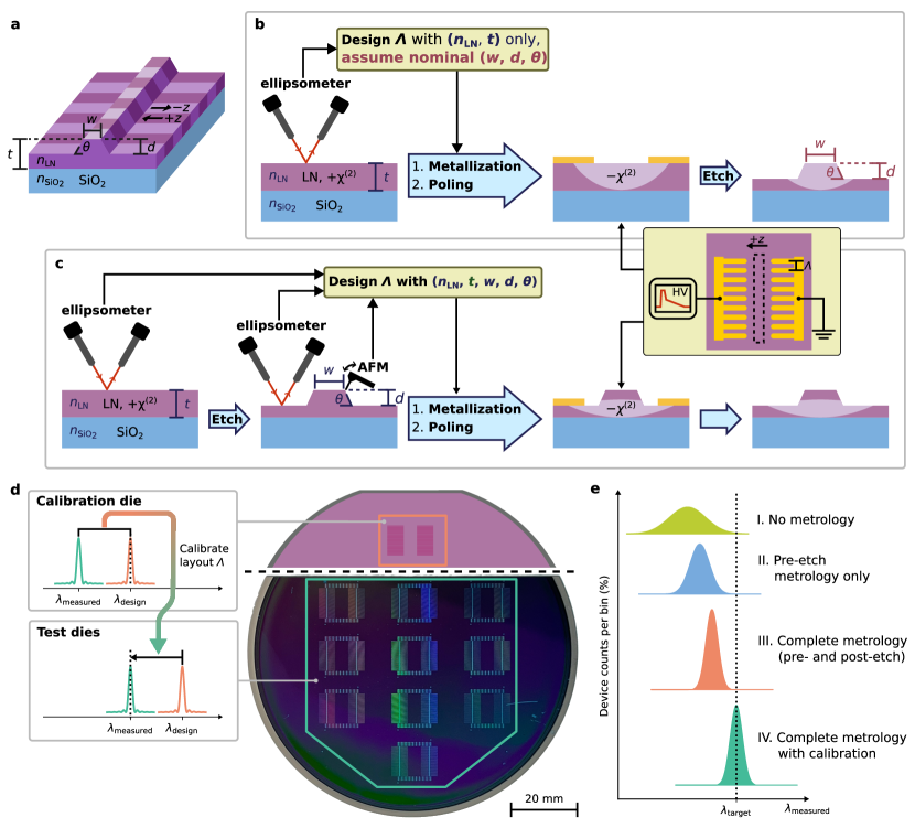
Recent advancements in thin-film lithium niobate (TFLN) photonics have led to a new generation of high-performance electro-optic devices, including modulators, frequency combs, and microwave-to-optical transducers. However, the broader adoption of TFLN-based devices that rely on all-optical nonlinearities have been limited by the sensitivity of quasi-phase matching (QPM), realized via ferroelectric poling, to fabrication tolerances. Here, we propose a scalable fabrication process aimed at improving the wavelength-accuracy of optical frequency mixers in TFLN. In contrast to the conventional pole-before-etch approach, we first define the waveguide in TFLN and then perform ferroelectric poling. This sequence allows for precise metrology before and after waveguide definition to fully capture the geometry imperfections. Systematic errors can also be calibrated by measuring a subset of devices to fine-tune the QPM design for remaining devices on the wafer. Using this method, we fabricated a large number of second harmonic generation devices aimed at generating 737 nm light, with 73% operating within 5 nm of the target wavelength. Furthermore, we also demonstrate thermo-optic tuning and trimming of the devices via cladding deposition, with the former bringing ~96% of tested devices to the target wavelength. Our technique enables the rapid growth of integrated quantum frequency converters, photon pair sources, and optical parametric amplifiers, thus facilitating the integration of TFLN-based nonlinear frequency mixers into more complex and functional photonic systems.
研究动机与目标
- 解决由于制造引起的几何变化导致的基于TFLN的非线性混频器波长不准确问题。
- 通过将极化与刻蚀解耦,实现准相位匹配(QPM)器件的晶圆级高精度制造。
- 通过基于波导几何测量的系统性误差校准,减少对试错设计的依赖。
- 展示可扩展的波长调谐与修整,以集成到复杂光子电路中。
- 为量子频率转换和光子对源等应用实现高良率、波长准确的器件。
提出的方法
- 该方法将传统的极化前刻蚀顺序反转,先通过干法刻蚀定义波导,再进行铁电极化。
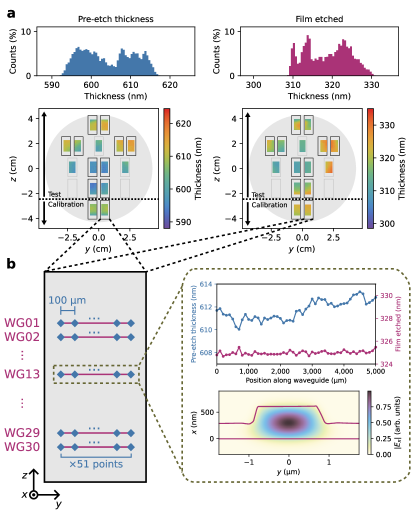
- 利用原子力显微镜(AFM)在晶圆多个位置测量刻蚀前后的薄膜厚度和波导几何形状。
- 基于测量的波导截面,计算具有局部变化的QPM光栅周期,以补偿几何缺陷。
- 通过测量部分器件的系统性误差,校准QPM设计参数,以调整晶圆上其余器件的参数。
- 通过外部陶瓷加热器施加热光调谐,实现120 °C范围内的工作波长移动。
- 采用SiO₂包层沉积进行波长修整,其蓝移速率随厚度增加而降低。
实验结果
研究问题
- RQ1能否通过将极化与刻蚀解耦的晶圆级制造工艺提升TFLN非线性混频器的波长精度?
- RQ2刻蚀前后的测量在多大程度上可减少QPM器件的波长偏差?
- RQ3基于测量器件几何形状的系统性误差校准能否提升晶圆上器件的良率与精度?
- RQ4热光调谐在修正高精度TFLN器件中残余波长误差方面的有效性如何?
- RQ5包层沉积能否提供一种可扩展、低损耗的非线性混频器工作波长精细调谐方法?
主要发现
- 经过系统性校准后,73%的二次谐波生成器件的工作波长在目标波长737 nm的±5 nm范围内。
- 热光调谐使工作波长最大移动12.1 nm,约96%的测试器件进入目标波长范围。
- SiO₂包层沉积导致工作波长蓝移超过100 nm,且随着厚度增加,调谐速率降低。
- 刻蚀前极化工艺通过基于局部波导几何形状测量的QPM光栅周期精确校准,相比传统方法显著减小了波长展宽。
- 该方法在两次晶圆工艺中均实现了高良率的波长准确器件,分别制造了600个和300个非校准器件。
- 高包层厚度下光谱展宽表明群速度失配增加,但对典型修整范围(<50 nm)影响甚微。
更好的研究,从现在开始
从阅读论文到最终审阅,大幅缩短您的研究时间。
无需绑定信用卡
本解读由 AI 生成,并经人工编辑审核。