
[论文解读] Femtosecond laser induced creation of G and W-centers in silicon-on-insulator substrates
本研究通过飞秒激光退火技术,在绝缘体上硅(SOI)衬底中实现了确定性、按需生成的W-中心和G-中心——基于硅的量子发射体。该方法获得的缺陷质量与传统离子注入技术相当,无需碳离子注入即可实现缺陷生成,并可通过低温退火选择性擦除G-中心,同时增强W-中心的发光,从而实现精确、局域化且低成本的量子发射体制造。
The creation of fluorescent defects in silicon is a key stepping stone towards assuring the integration perspectives of quantum photonic devices into existing technologies. Here we demonstrate the creation, by femtosecond laser annealing, of W and G-centers in commercial silicon on insulator (SOI) previously implanted with 12C+ ions. Their quality is comparable to that found for the same emitters obtained with conventional implant processes; as quantified by the photoluminescence radiative lifetime, the broadening of their zero-phonon line (ZPL) and the evolution of these quantities with temperature. In addition to this, we show that both defects can be created without carbon implantation and that we can erase the G-centers by annealing while enhancing the W-centers' emission. These demonstrations are relevant to the deterministic and operando generation of quantum emitters in silicon.
研究动机与目标
- 开发一种与现有光子学和电子集成平台兼容的、确定性且低成本的SOI衬底中硅基量子发射体的制备方法。
- 证明飞秒激光退火可生成光学特性与传统离子注入方法相当的W-和G-中心。
- 探究在SOI中通过该激光方法生成G-和W-中心是否需要碳离子注入。
- 探索通过辐照后热处理实现G-中心选择性擦除及W-中心发光增强的可能性。
提出的方法
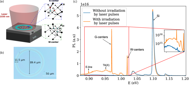
- 使用焦距为750 mm的平凸透镜,将波长为1030 nm、脉宽小于200 fs、重复频率为1 kHz的飞秒激光脉冲聚焦于SOI晶圆上,实现局部热退火。
- 样品在95–218 µJ的能量下接受1–5个脉冲辐照,在220 nm厚的顶层硅层中产生缺陷。
- 使用了两种类型的SOI衬底:一种为在34 keV能量下注入12C+离子、剂量为1×10¹²和1×10¹³ cm⁻²的样品,另一种为含有残余碳的原始SOI衬底。
- 在辐照后对样品进行125 °C、5分钟的退火处理,以研究缺陷演化过程及选择性擦除G-中心。
- 在12 K下使用405 nm连续波泵浦激光和配备InGaAs探测器(波长范围900–1600 nm)的光谱仪进行光致发光(PL)测量。
- 采用时间分辨PL和温度依赖PL分析辐射寿命、零声子线(ZPL)展宽以及ZPL的热红移。
实验结果
研究问题
- RQ1飞秒激光退火是否可用于在SOI衬底中生成光学特性与标准离子注入方法相当的W-和G-中心?
- RQ2通过该激光方法在SOI中生成G-和W-中心是否需要碳离子注入?
- RQ3低温退火是否可选择性擦除G-中心,同时增强W-中心的发光?
- RQ4该激光工艺是否能够实现硅中量子发射体的确定性、按需且空间受限的生成?
主要发现
- 通过飞秒激光退火生成的W-和G-中心的光致发光辐射寿命、ZPL展宽以及温度依赖的ZPL位移,与文献中报道的传统制备缺陷的特性相当。
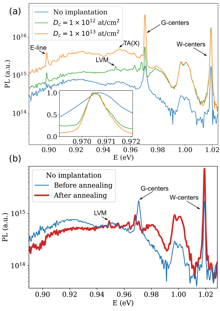
- 在未进行任何碳离子注入的原始SOI衬底中,成功生成了G-和W-中心,表明晶圆中残余的碳已足以支持缺陷形成。
- 在未注入样品中,G-中心的ZPL线宽更宽且发生蓝移,与较低的内部应力和缺陷密度一致。
- 低温退火(125 °C,5分钟)选择性地擦除了G-中心,同时略微增强了W-中心的PL发射强度,与先前研究的预期相反。
- 缺陷生成的空间局域性与激光光斑尺寸(约178 µm束腰)一致,实现了局域化,甚至可能实现单缺陷工程。
- 该方法可在无需离子注入的情况下,实现确定性、按需且区域受限的W-中心生成,为量子光子集成提供了一种可扩展且成本效益高的替代方案。
更好的研究,从现在开始
从阅读论文到最终审阅,大幅缩短您的研究时间。
无需绑定信用卡
本解读由 AI 生成,并经人工编辑审核。