
[논문 리뷰] Bright and pure single-photon source in a silicon chip by nanoscale positioning of a color center in a microcavity
이 논문은 SOI에서 원형 브래그 포착 공진계에 W 중심을 결정론적으로 위치시켜 모든 실리콘 소자 기반의 칩온 칩 단일 광자원을 제시하며, CW 및 펄스 여기에서 탁월한 단일 광자 순도와 함께 Purcell-향상된 ZPL 방출을 달성합니다.
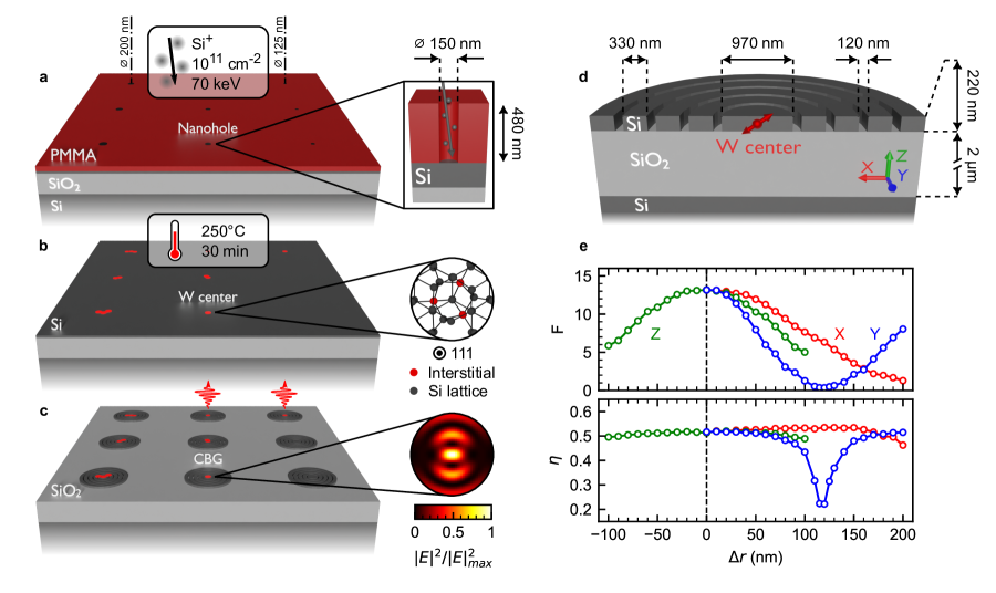
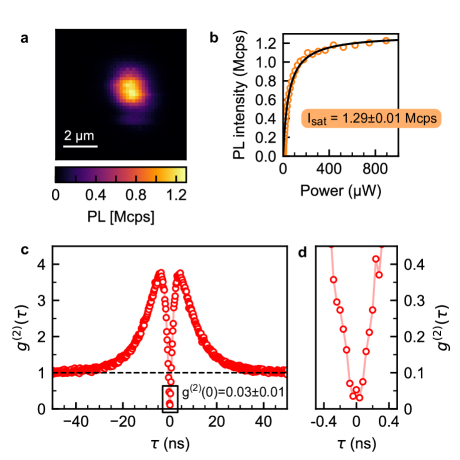
We present an all-silicon source of near-infrared linearly-polarized single photons, fabricated by nanoscale positioning of a color center in a silicon-on-insulator microcavity. The color center consists of a single W center, created at a well-defined position by Si$^{+}$ ion implantation through a 150 nm-diameter nanohole in a mask. A circular Bragg grating cavity resonant with the W's zero-phonon line at 1217 nm is fabricated at the same location as the nanohole. By Purcell enhancement of zero-phonon emission, we obtain a photon count rate of $1.29 \pm 0.01$ Mcounts/s at saturation under above-gap continuous-wave excitation with a Debye-Waller factor of $98.6\pm1.4 \%$. A clean photon antibunching behavior is observed up to pump powers ensuring saturation of the W's emission ($g^{(2)}(0)=0.06\pm0.02$ at $P=9.2P_{sat}$), evidencing that the density of additional parasitic fluorescent defects is very low. We also demonstrate the triggered emission of single photons with $93\pm2 \%$ purity under weak pulsed laser excitation. At high pulsed laser power, we reveal a detrimental effect of repumping processes, that could be mitigated using selective pumping schemes in the future. These results represent a major step towards on-demand sources of indistinguishable near-infrared single photons within silicon photonics chips.
연구 동기 및 목표
- 실리콘에서 나노스케일 발광체 위치지정을 사용해 밝고 순수한 단일 광자의 결정론적 온칩 생성 시연.
- 원형 브래그 격자 공진기에 있는 W 센터의 제로 포논선(ZPL) 방출에 대한 강한 Purcell 증가 달성.
- CW 및 펄스 전 excited에서 단일 광자 순도, 밝기, 편광 특성 평가.
- 실리콘 포토닉스에서 대규모로, 구분 가능한(on-chip indistinguishable) 광자원의 가능성과 한계 평가.
제안 방법
- PMMA 마스크의 150 nm 나노구멍을 통한 Si+ 이온 주입으로 W 센터 배열 제작.
- 나노홀 위치에 중심을 둔 원형 브래그 격자(CBG) 공진기 생성 및 W ZPL 1217–1218 nm에 공진.
- 상한-갭 CW 및 펄스 전 excited에서 광발광 분광법 및 2차 상관 g(2)(τ)를 이용한 방출 특성화.
- 반사율 측정을 통해 공진기 Q 인자와 Purcell 증가를 추출하여 공진-발광자 결합 분석.
- 펄스 펌핑하에서 삶주기(lifetime) 측정을 통해 제로-포논선(ZPL) 분율과 Purcell-향상 방사 붕괴 추정.
실험 결과
연구 질문
- RQ1칩 내 실리콘 광포학 구조에서 공진기 안티노드에 단일 W 센터를 결정론적으로 배치하여 Purcell 증가를 최대화할 수 있는가?
- RQ2CW 및 펄스 전 excited에서 SOI CBG 공진기에서 W-센터의 밝기, 순도(g(2)(0)), ZPL 분율은 무엇인가?
- RQ3발출체-공진기 이격(detuning) 및 위치 정합 오차가 이 시스템의 수집 효율과 Purcell 팩터에 어떤 영향을 미치는가?
- RQ4비발광 상태 등 블링킹 문제와 실리콘 색이 센터의 칩상으로 구별 가능한 단일 광자 방출 개선의 주요 한계 및 전망은 무엇인가?
주요 결과
- W 센터가 공진기 안테노드와 정렬된 위치에 결정론적으로 생성되어 ZPL 방출의 강한 Purcell 증가를 달성.
- CW 포화 카운트 속도 약 1.29 Mcps, g(2)(0) ≈ 0.03–0.06 전체 전력 범위에서 관측, 매우 낮은 기생 방출을 나타냄.
- 제로 포논 방출 분율은 PL의 약 98.6%로, 공진기 Purcell 증가에 의한 ZPL 방출의 효율성을 나타냄.
- 강한 순도 높은 편광 단일 광자원을 약한 펄스 펌핑하에서 시연, 트리거 방출의 순도 93% 달성.
- 공진기 반사율 측정은 Q ≈ 158(Δλ ≈ 7.7 nm)인 모드를 보여주며, 시뮬레이션과 근접한 spectral alignment를 나타냄.
- 펄스 전 excited에서 트리거 방출은 단일 광자 방출에 해당하는 중심 피크 영역을 가진 반-집합(bunched) 억제를 보였고, blinking(준상태 다이나믹스)이 관찰되고 분석됨.
- 무패턴 SOI W 센처 대비 큰 향상을 보여줌( 포화에서 PL 카운트 속도 약 400배 향상), 공진기가 밝기에 기여하는 역할 강조.
더 나은 연구,지금 바로 시작하세요
논문 읽기부터 검토까지, 연구 시간을 획기적으로 줄여보세요.
카드 등록 없음 · 무료 플랜 제공
이 리뷰는 AI가 만들고, 인간 에디터가 검토했습니다.