[논문 리뷰] 3D photonics for ultra-low energy, high bandwidth-density chip data links
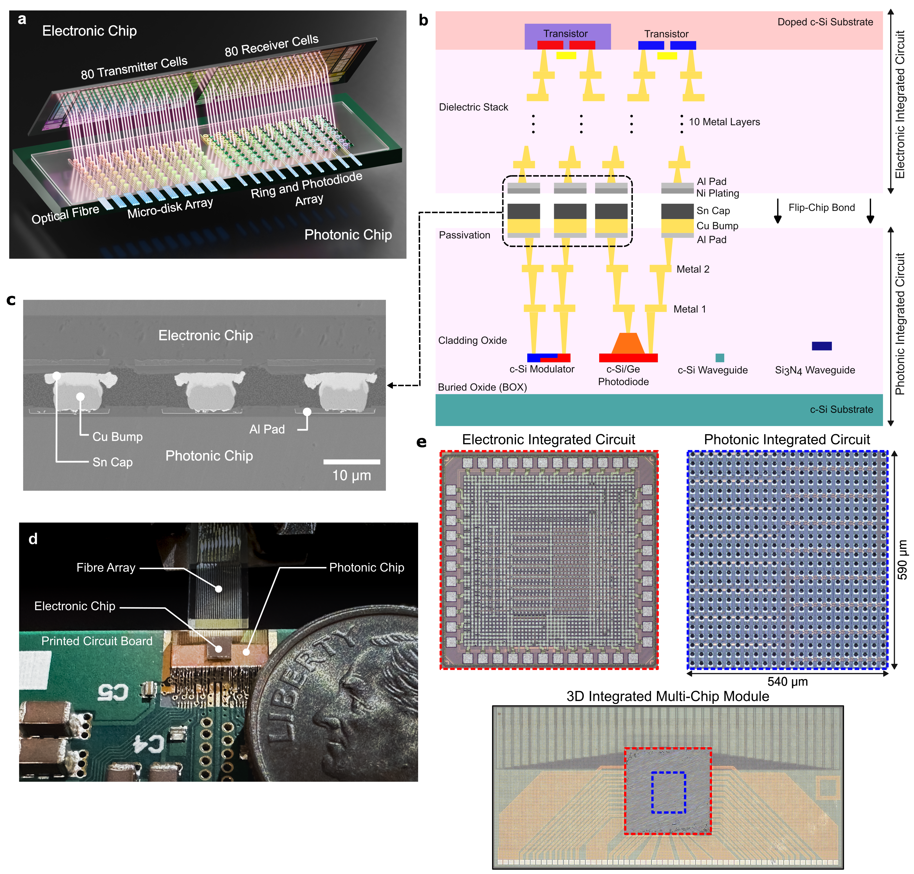
80개의 송신 채널과 80개의 수신 채널을 갖춘 3D 통합 광전자 트랜시버를 시연하여 총 800 Gb/s 및 5.3 Tb/s/mm^2 대역폭 밀도를 달성하고 약 120 fJ/비트 수준에서, 저-용량 3D 본딩 및 CMOS-포토닉스 공설계(co-design)를 사용.
Artificial intelligence (AI) hardware is positioned to unlock revolutionary computational abilities across diverse fields ranging from fundamental science [1] to medicine [2] and environmental science [3] by leveraging advanced semiconductor chips interconnected in vast distributed networks. However, AI chip development has far outpaced that of the networks that connect them, as chip computation speeds have accelerated a thousandfold faster than communication bandwidth over the last two decades [4, 5]. This gap is the largest barrier for scaling AI performance [6, 7] and results from the disproportionately high energy expended to transmit data [8], which is two orders of magnitude more intensive than computing [9]. Here, we show a leveling of this long-standing discrepancy and achieve the lowest energy optical data link to date through dense 3D integration of photonic and electronic chips. At 120 fJ of consumed energy per communicated bit and 5.3 Tb/s bandwidth per square millimeter of chip area, our platform simultaneously achieves a twofold improvement in both energy consumption and bandwidth density relative to prior demonstrations [10, 11]. These improvements are realized through employing massively parallel 80 channel microresonator-based transmitter and receiver arrays operating at 10 Gb/s per channel, occupying a combined chip footprint of only 0.32 mm2. Furthermore, commercial complementary metal-oxide-semiconductor (CMOS) foundries fabricate both the electronic and photonic chips on 300 mm wafers, providing a clear avenue to volume scaling. Through these demonstrated ultra-energy efficient, high bandwidth data communication links, this work eliminates the bandwidth bottleneck between spatially distanced compute nodes and will enable a fundamentally new scale of future AI computing hardware without constraints on data locality.
연구 동기 및 목표
- 칩 연산 속도와 인터커넥트 대역폭 간의 격차를 줄여 AI 하드웨어의 데이터 전송 병목을 해소한다.
- Dense하게 통합된 광학 및 전자 칩을 3D 스택으로 사용하여 에너지 효율적이고 고대역폭의 칩 간 통신을 시연한다.
- 실용적이고 대량 확장 가능한 포토닉 링크를 가능하게 하기 위해 채널당 에너지를 최소화하면서 데이터 채널 수를 확장한다.
- 대규모 배치를 위해 300 mm 웨이퍼에서 CMOS 제조 포토닉-전자 트랜시버의 실현 가능성을 보인다.
제안 방법
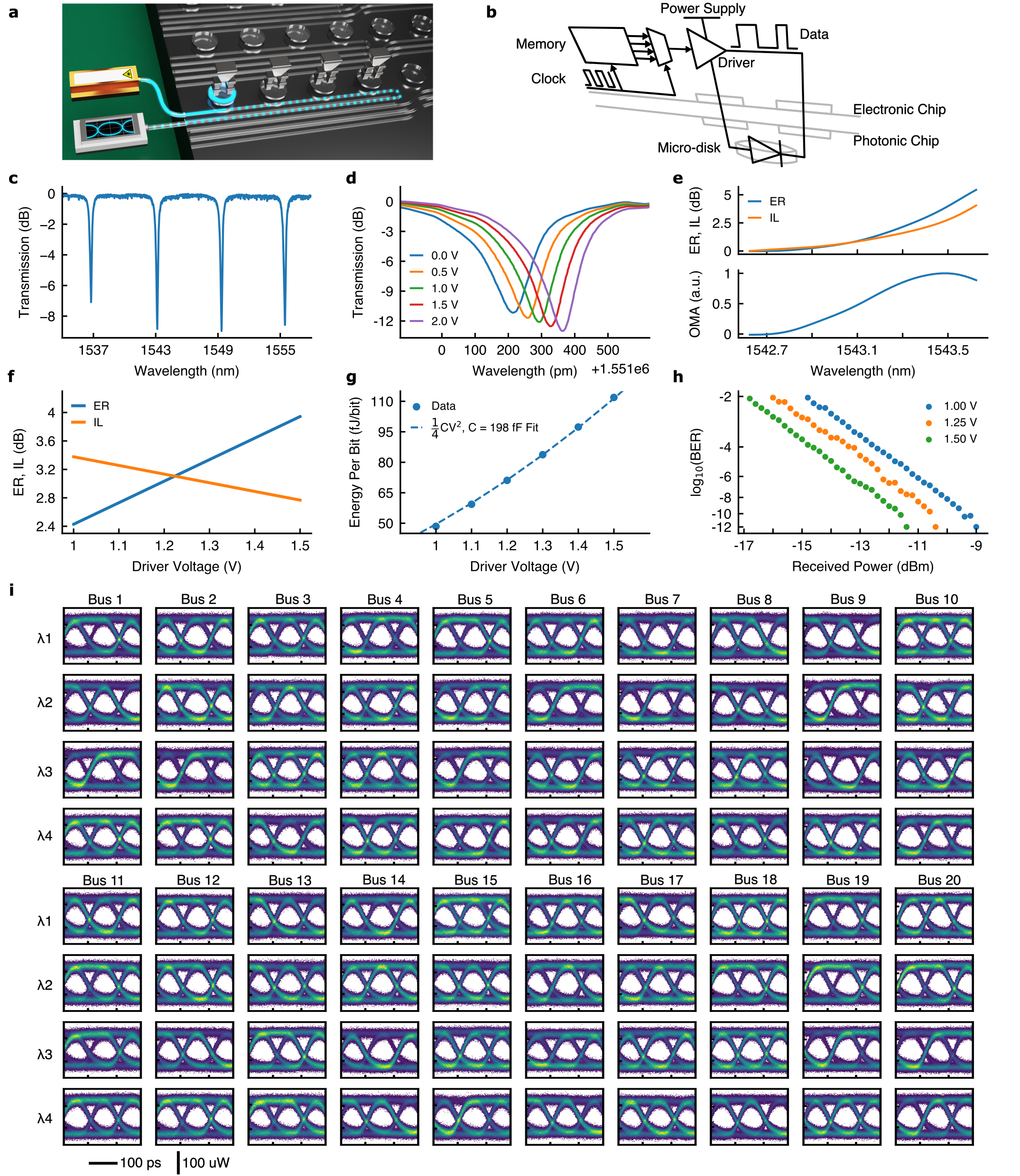
- 20 개의 웨이브가이드 버스에 4개의 파장을 버스당 배치하여 80 송신 셀과 80 수신 셀로 구성된 3D 통합 트랜시버를 개발한다.
- 광학 및 전자 칩 간 고밀도 결합을 위한 15 μm 간격의 구리 기둥 범프와 10 μm 범프 직경(25 μm 피치)을 사용한다.
- 저용량 포토닉 소자와 CMOS 드라이버를 공설계하여 송신기 배열의 용량 약 ~200 fF, 수신기 에너지 약 ~70 fJ/비트를 달성한다.
- 각 송신기를 채널당 10 Gb/s로 작동시켜 80 채널에서 총 800 Gb/s를 달성하고, 송신기 단일 칩 면적은 0.32 mm^2이며, 배열 전체 면적은 0.32 mm^2 이다.
- Miller 1/4 CV^2 모델을 사용하여 비트당 에너지를 특성화하고 송신기 및 수신기 성능 주변의 채널당 에너지를 측정한다.
- 특정 광 파워 조건에서 4 채널 파장을 갖는 독립적인 트랜시버를 통한 완전한 송신기-수신기 간 광 데이터 링크를 시연하고 BER 성능을 10^-12까지 달성한다.
실험 결과
연구 질문
- RQ1 densely integrated 3D photonic-electronic transceiver at chip scale에서 달성 가능한 에너지-비트 및 대역폭 밀도는 무엇인가?
- RQ2고 채널 수(80x80) 트랜시버가 채널당 에너지를 낮추면서도 높은 총 데이터 속도를 유지할 수 있는가?
- RQ3채널 밀도를 최대화하면서 신뢰성이나 BER를 해치지 않는 본딩 및 소자 설계 선택은 무엇인가?
- RQ4전체 송신기-수신기 링크에서 통합된 3D 포토닉-전자 링크의 실용적 BER 성능과 감도는 어떠한가?
주요 결과
- 80채널 송신 배열과 80채널 수신 배열이 0.32 mm^2(송신기) 면적에서 총 800 Gb/s 및 5.3 Tb/s/mm^2 대역폭 밀도를 달성한다.
- 송신기는 전체 링크에 대해 120 fJ/비트를 소모하고 수신기는 10 Gb/s 작동에서 70 fJ/비트를 소모하며, 전체 송신기-수신기 링크 에너지는 약 120 fJ/비트이다.
- 정전용량 예산(패드, 범프, 마이크로 디스크, 포토다이오드 및 드라이버)은 송신기 정전용량 약 199 fF로 측정된 비트당 에너지와 일치한다.
- 4채널을 이용한 완전한 송신기-수신기 광 링크는 테스트 조건에서 BER이 <= 6×10^-8를 시연하고 채널 간 오픈 아이 다이어그램을 보여준다.
- 15 μm 간격과 10 μm 범프 직경(25 μm 피치)을 이용한 본딩은 강건한 2.1 kg 다이-투-다이 본드를 제공하고 기생 파라시틱을 낮춰 고밀도 통합을 가능하게 한다.
- 데이터 링크는 4채널 레이저 소스와 4개의 파장을 사용하여 기능을 시연하고, 유리한 조건에서 BER이 약 10^-12에 가깝다.
더 나은 연구,지금 바로 시작하세요
연구 설계부터 논문 작성까지, 연구 시간을 획기적으로 줄여보세요.
카드 등록 없음 · 무료 플랜 제공
이 리뷰는 AI가 만들고, 인간 에디터가 검토했습니다.