[論文レビュー] 3D photonics for ultra-low energy, high bandwidth-density chip data links
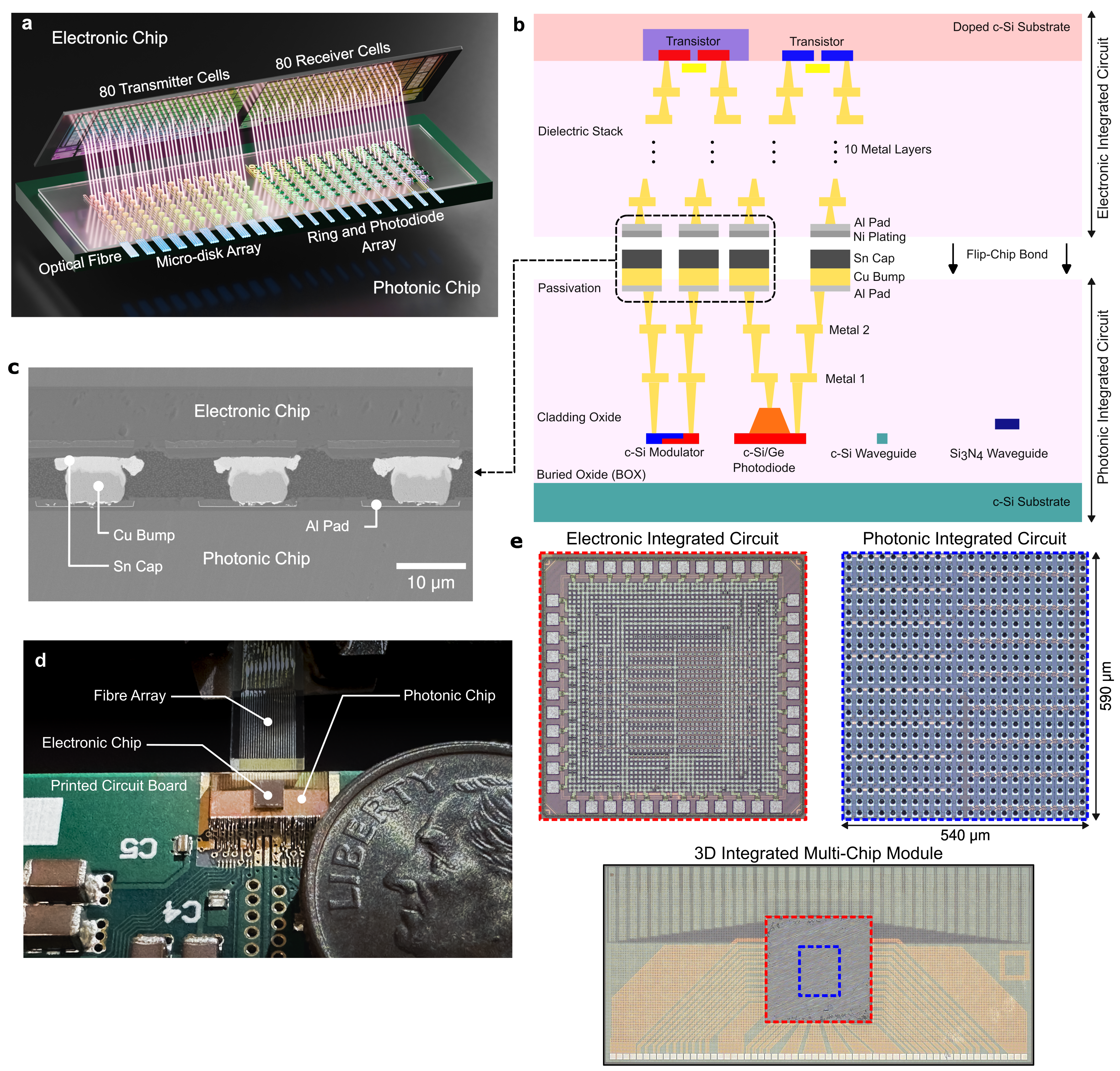
3D統合フォトニック-エレクトリックトランシーバを実証。80送信チャネルと80受信チャネルで総計800 Gb/s、帯域密度5.3 Tb/s/mm^2、約120 fJ/bit、低容量3D結合とCMOS-フォトニクス共設計を用いる。
Artificial intelligence (AI) hardware is positioned to unlock revolutionary computational abilities across diverse fields ranging from fundamental science [1] to medicine [2] and environmental science [3] by leveraging advanced semiconductor chips interconnected in vast distributed networks. However, AI chip development has far outpaced that of the networks that connect them, as chip computation speeds have accelerated a thousandfold faster than communication bandwidth over the last two decades [4, 5]. This gap is the largest barrier for scaling AI performance [6, 7] and results from the disproportionately high energy expended to transmit data [8], which is two orders of magnitude more intensive than computing [9]. Here, we show a leveling of this long-standing discrepancy and achieve the lowest energy optical data link to date through dense 3D integration of photonic and electronic chips. At 120 fJ of consumed energy per communicated bit and 5.3 Tb/s bandwidth per square millimeter of chip area, our platform simultaneously achieves a twofold improvement in both energy consumption and bandwidth density relative to prior demonstrations [10, 11]. These improvements are realized through employing massively parallel 80 channel microresonator-based transmitter and receiver arrays operating at 10 Gb/s per channel, occupying a combined chip footprint of only 0.32 mm2. Furthermore, commercial complementary metal-oxide-semiconductor (CMOS) foundries fabricate both the electronic and photonic chips on 300 mm wafers, providing a clear avenue to volume scaling. Through these demonstrated ultra-energy efficient, high bandwidth data communication links, this work eliminates the bandwidth bottleneck between spatially distanced compute nodes and will enable a fundamentally new scale of future AI computing hardware without constraints on data locality.
研究の動機と目的
- AIハードウェアにおけるデータ転送ボトルネックを解消するため、チップ計算速度とインターコネクト帯域幅のギャップを埋める。
- 3Dスタックで密に統合されたフォトニックおよび電子チップを用いたエネルギー効率の高い、帯域幅の大きいチップ間通信を実証する。
- データチャネル数を拡張しつつ、チャネルあたりのエネルギーを最小化して現実的で体積スケーラブルなフォトニックリンクを可能にする。
- 大規模展開のための300 mmウェハ上でCMOS製造のフォトニック-エレクトロニックトランシーバの実現性を示す。
提案手法
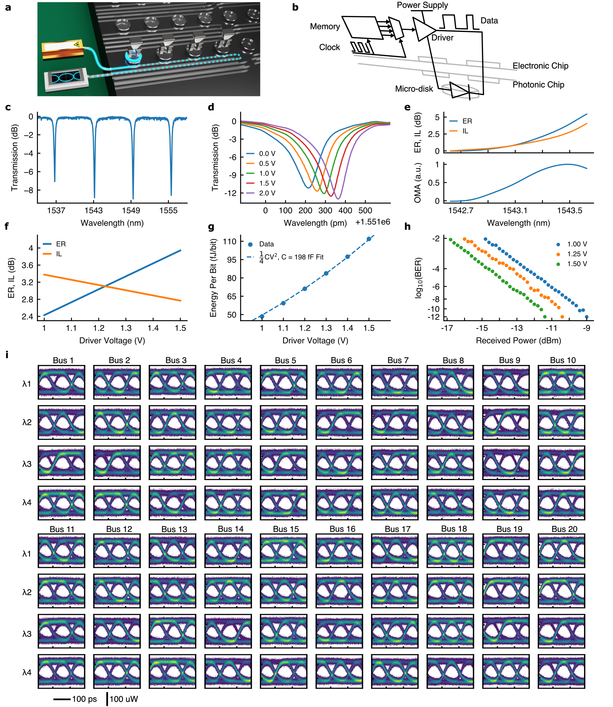
- 80送信セルと80受信セルを20のウェーブガイドバスに4波長ずつ配置した3D統合トランシーバを開発する。
- フォトニックチップと電子チップ間の高密度結合のために、15 μm間隔の銅ピラーボンプと10 μmボンプ直径(25 μmピッチ)を使用する。
- 低容量のフォトニックデバイスとCMOSドライバを共設計し、送信器約200 fF、受信器約70 fJ/bitを達成する。
- 各チャネルを80チャネル全体で10 Gb/sで動作させ、0.32 mm^2の送信器面積およびアレイ全体で0.15 mm^2(送信器)/0.32 mm^2のエリアを達成して総計800 Gb/sとする。
- ボルムの Miller 1/4 CV^2 モデルを用いてエネルギー/bitを評価し、送信側および受信側の性能で1チャネルあたりのエネルギーを測定する。
- 4波長チャネルを用いた完全な送信機-受信機間の光データリンクをデモンストレーションし、特定の光パワー条件下でBER性能を10^-12レベルまで達成。
実験結果
リサーチクエスチョン
- RQ1集積3Dフォトニック-エレクトロニックトランシーバにおけるチップ規模での達成可能なエネルギー/bitと帯域密度はどれくらいか。
- RQ2高チャネル数(80x80)トランシーバは、低いチャネルあたりエネルギーを維持しつつ高い総データレートを達成できるか。
- RQ3チャネル密度を最大化しつつ信頼性やBERを損なわない結合設計とデバイス設計の選択は何か。
- RQ4完全な送信機-受信機リンクを横断する統合3Dフォトニック-エレクトロニックリンクの実用的なBER性能と感度はどの程度か。
主な発見
- 80チャネル送信アレイと80チャネル受信アレイが0.32 mm^2(送信器)領域で総計800 Gb/sと帯域密度5.3 Tb/s/mm^2を達成。
- 送信器は全リンクで120 fJ/bit、受信器は10 Gb/s動作時に70 fJ/bit、送信機-受信機リンク全体で約120 fJ/bitのエネルギーを消費。
- パッド、バンプ、マイクロディスク、フォトダイオード、ドライバを含む容量予算は約199 fFの送信容量となり、測定エネルギー/bitと整合。
- 4チャネルを用いた完全な送信機-受信機光リンクは、BERが tested conditionsで<=6×10^-8となり、チャネル全体でオープンアイダイアグラムを示す。
- 15 μm間隔と10 μmボンプ直径(25 μmピッチ)の結合は堅牢な2.1 kgダイ間結合と低寄生成分を提供し、高密度統合を実現。
- データリンクは4チャネルレーザー源と4波長で機能し、有利な条件下でBERを約10^-12近くまで達成。
より良い研究を、今すぐ始めましょう
論文設計から論文執筆まで、研究時間を劇的に削減しましょう。
クレジットカード登録不要
このレビューはAIが作成し、人間の編集者が確認しました。