[論文レビュー] Origin and magnitude of 'designer' spin-orbit interaction in graphene on semiconducting transition metal dichalcogenides
本論文は、半導体的遷移金属ジ chalcogenide (TMD) 上に形成されたグラフェンが、~0.2 psという非常に短いスピン緩和時間を示す、超強力で頑丈かつ界面に起因するスピン軌道相互作用 (SOI) を示すことを実証している。このSOIは不純物に起因するのではなく、バンド構造の変化に起因しており、ゲート駆動可能なシュビニコフ=ド・ハース (Shubnikov-de Haas) 力学的抵抗振動の測定により、約10 meVの分裂が確認され、グラフェン/TMDはスピン・バルク効果およびバルク効果の実現に有望なプラットフォームである。
We use a combination of experimental techniques to demonstrate a general occurrence of spin-orbit interaction (SOI) in graphene on transition metal dichalcogenide (TMD) substrates. Our measurements indicate that SOI is ultra-strong and extremely robust, despite it being merely interfacially-induced, with neither graphene nor the TMD substrates changing their structure. This is found to be the case irrespective of the TMD material used, of the transport regime, of the carrier type in the graphene band, and of the thickness of the graphene multilayer. Specifically, we perform weak antilocalization measurements as the simplest and most general diagnostic of SOI, and show that the spin relaxation time is very short in all cases regardless of the elastic scattering time. Such a short spin-relaxation time strongly suggests that the SOI originates from a modification of graphene band structure. We confirmed this expectation by measuring a gate-dependent beating, and a corresponding frequency splitting, in the low-field Shubnikov-de Haas magneto-resistance oscillations in high quality bilayer graphene on WSe$_2$. These measurements provide an unambiguous diagnostic of a SOI-induced splitting in the electronic band structure, and their analysis allows us to determine the SOI coupling constants for the Rashba term and the so-called spin-valley coupling term, i.e., the terms that were recently predicted theoretically for interface-induced SOI in graphene. The magnitude of the SOI splitting is found to be on the order of 10 meV, more than 100 times greater than the SOI intrinsic to graphene. Both the band character of the interfacially induced SOI, as well as its robustness and large magnitude make graphene-on-TMD a promising system to realize and explore a variety of spin-dependent transport phenomena, such as, in particular, spin-Hall and valley-Hall topological insulating states.
研究の動機と目的
- グラフェン/半導体的遷移金属ジカルコゲナイド (TMD) 上における「デザイナー型」スピン軌道相互作用 (SOI) の起源と大きさを特定すること。
- 観測されたSOIが、さまざまなTMD材料およびグラフェンの構造的条件下で普遍的かつ頑丈な現象であるかどうかを確立すること。
- これらのヘテロ構造において、不純物駆動型とバンド構造駆動型のSOIメカニズムを区別すること。
- 輸送測定を用いて、誘導されたSOIにおけるラシュバ項およびスピンバルク結合項の強度を定量すること。
- グラフェン/TMDがスピンホールおよびバルクホールトポロジカル状態を実現するためのプラットフォームとしての可能性を調査すること。
提案手法
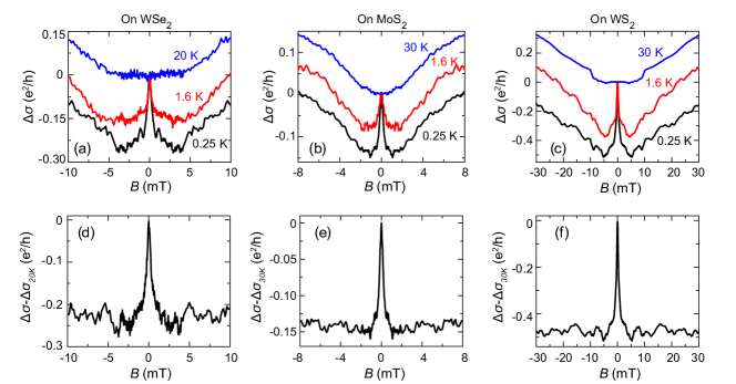
- スピン緩和時間の抽出によりスピン軌道結合の強度を調べる弱い反局在 (WAL) 測定を実施する。
- WSe₂上に形成された高品質な二層グラフェンにおけるゲート依存性を持つシュビニコフ=ド・ハース (SdH) 磁気抵抗振動を測定し、バンド構造の分裂を検出する。
- SdH振動の周波数分裂を分析して、ラシュバおよびスピンバルク結合定数を抽出する。
- スピン軌道項を含むディラックハミルトニアンに基づく理論的モデルを用いて実験データを解釈する。
- 異なる弾性散乱時間を持つデバイス間でスピン緩和時間を比較し、内在的SOI効果を分離する。
- Hikami-Larkin-Nagaoka (HLN) 公式をWALデータにフィットさせ、スピン緩和時間 τ_so を抽出する。
実験結果
リサーチクエスチョン
- RQ1グラフェン/TMD基板上における超強力なスピン軌道相互作用の微視的起源は何か?
- RQ2観測されたスピン軌道結合は、TMD材料、キャリア型、グラフェンの厚さに依存しない、グラフェン/TMDヘテロ構造の普遍的特徴であるか?
- RQ3スピン軌道相互作用はバンド構造の変化に起因するのか、それとも不純物散乱に起因するのか?
- RQ4グラフェン-TMD界面に誘導されたラシュバ項およびスピンバルク結合項の定量的値は何か?
- RQ5電気的ゲーティングによって誘導されたSOIの強度を調整可能か?そしてこれはトポロジカルスピントロニクスデバイスへの意味をどのように示唆するか?
主な発見
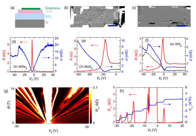
- すべてのデバイスにおいてスピン緩和時間 τ_so が一貫して ≤ 0.2 ps であり、弾性散乱時間に依存しないことから、頑丈で内在的なSOIメカニズムであることが示された。
- τ_so が弾性散乱時間の変動にかかわらず短いまま維持されることから、SOIは不純物駆動型ではなく、実験的に確認された。
- WSe₂上に形成された二層グラフェンにおけるゲート依存性SdH振動は、約10 meVの周波数分裂を示し、SOIに起因するバンド構造の変化を直接的証明した。
- ラシュバおよびスピンバルク結合項が定量的に抽出され、界面に起因するSOIにおけるその役割が確認された。
- SOI分裂の大きさは約10 meVであり、グラフェンの内在的SOIを100倍以上上回る。
- SOIはさまざまなTMD材料、キャリア型、グラフェン多層膜の厚さにわたり普遍的であり、界面特有の効果であることが示された。
より良い研究を、今すぐ始めましょう
論文設計から論文執筆まで、研究時間を劇的に削減しましょう。
クレジットカード登録不要
このレビューはAIが作成し、人間の編集者が確認しました。